
HALT Testing: HALT and HASS Testing for PCB Assembly Reliability
Two acronyms dominate accelerated reliability work on electronics, and they answer different questions. HALT testing asks how much abuse a design can take before it breaks, while HASS testing asks whether a production unit was built correctly. Used together they shorten the path from a prototype to a qualified product, but each has limits that are easy to overlook. This article explains how both are run and what the results actually mean.
What HALT and HASS Actually Test
Highly accelerated life testing is a development tool. It applies stresses well beyond the specified operating range, one at a time and then in combination, until the product fails. The purpose is not to simulate field life but to find the weakest link and to measure how much margin exists between the specification and that link. A design that fails at 40 degrees above its rating has little margin; one that fails at 90 degrees above has a great deal.
Highly accelerated stress screening is a production tool. It applies a stress level that is known from the HALT results to be safely below the destruct limit, and it is applied to every unit in a batch to precipitate latent defects such as a poor solder joint, a marginal via, or a contaminated connector. Units that fail the screen are repaired or scrapped, and the failures are fed back to the process rather than to the design.
Step-Stress Methodology
A HALT programme usually begins with a cold step stress, then a hot step stress, then rapid thermal cycling, then vibration, and finally a combined environment. Each step raises the stress by a fixed increment and holds it for a dwell period long enough for the assembly to reach equilibrium, with a functional test between steps. The first step at which the unit fails is recorded as the operating limit, and the stress is then reduced to verify recovery.
Two limits are recorded for each stress: the soft limit, where the unit stops working but recovers when the stress is removed, and the hard limit, where damage is permanent. The gap between the specification and the operating limit is the design margin. Every failure should be analysed to the component or joint that caused it, because the value of the test lies in the failure mechanism, not in the number.
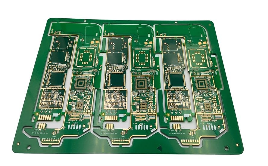
Thermal Step Stress in Practice
Thermal step stress uses an air chamber with a wide range, typically minus 60 to plus 150 degrees Celsius or beyond for industrial work. Ramp rates of 30 to 60 degrees per minute are common, which is far faster than a reflow profile and much faster than most field environments. Dwell times of 10 to 15 minutes let the assembly stabilise, and power is usually applied so that self-heating is part of the stress.
Thermal cycling with a fast ramp is the most damaging part of the sequence for solder joints and plated barrels, because it drives the coefficient of thermal expansion mismatch between materials. The same test is useful during production validation, where a shorter profile is applied to a sample rather than to every unit. Chamber loading matters: a board placed near the airflow path heats faster than one in a corner, so positions should be recorded and rotated.
Temperature alone rarely explains a failure, so each cycle should be paired with a functional test and, where possible, with in-situ monitoring of a daisy chain or a critical net. Continuous monitoring detects intermittent opens that a test at the end of a dwell would miss, which is exactly the class of defect that accelerated testing is meant to expose.
Vibration and Combined Environments
Vibration step stress uses a shaker table with random or swept-sine input, increasing the level until the assembly reaches its destruct limit. Boards are usually mounted in a fixture that reproduces the stiffness of the real enclosure, because a board that is bolted at four corners behaves very differently from one clipped along an edge. Accelerometers on the board, not on the table, record the actual input and the response of the structure.
Combined environments are where HALT becomes realistic. Applying thermal cycling and vibration at the same time finds failures that neither stress produces alone, particularly on large components with heavy bodies and on connectors that rely on a friction fit. The combination also reduces the number of test hours required, which is the main reason it is used in development schedules.
Fixture design deserves attention that it often does not receive. A fixture that damps the board hides the failure mode the test was designed to find, while one that is too stiff creates artificial stress concentrations at the mounting holes. Where the intent is to evaluate the assembly rather than the fixture, the same fixture should also be used for the qualification builds so that results can be compared between lots.

Interpreting Failures and Design Margin
A HALT report is only useful when each failure has a mechanism attached. A cracked solder joint on a ceramic capacitor points to thermal expansion mismatch and a need for compliant terminations or a different placement. A lifted pad points to a laminate or surface finish issue. An oscillating clock points to a component that is being pushed beyond its temperature range. The corrective action follows from the mechanism, not from the failure temperature alone.
Margin should also be reported as a ratio to the specification, not just as a difference. A product rated from 0 to 70 degrees that operates to 100 degrees has roughly 40 degrees of upper margin, but a component rated to 105 degrees has very little of its own margin left. Comparing the assembly limit with the component limits identifies which part will be the constraint if the specification is later widened.
From HALT to HASS Screens
A HASS profile is derived by taking the HALT limits and reducing them, commonly to about half of the difference between the operating limit and the specification. That leaves room for unit-to-unit variation and for measurement error while still precipitating process defects. The profile should then be validated by running known-good units through it and confirming that none fail, and by running seeded defects through it to confirm that they do.
Screens cost money and time, so the benefit has to be justified. The usual argument is that a screen catches escapes that functional test cannot detect, particularly intermittent joints and marginal plated vias. The usual counter-argument is that an aggressive screen can damage good product. Both are settled by data: track screen fallout, analyse the failures, and reduce the profile when the fallout rate drops to a level that no longer justifies the cycle time.
Limitations at Assembly Level
Accelerated testing at assembly level cannot cover every failure mechanism. Wear-out mechanisms such as electrolytic capacitor drying, connector fretting, and metal migration follow time-based physics that a short accelerated test does not reproduce faithfully. Contamination and corrosion need humidity with bias, which is a separate test rather than a step in the thermal sequence.
It is also easy to over-interpret a single passing run. A sample of one or two boards that survives the full profile demonstrates that the design is not obviously weak, not that it has a quantified margin. A meaningful programme uses enough units to show repeatability, documents every change to the fixture and the profile, and treats each result as evidence about a mechanism rather than as a certificate.
FAQ
Can HALT results be used as a reliability prediction? Not directly. HALT proves that a design has or lacks margin; converting a failure temperature into a field life figure requires a physics-based model and a known field stress profile.
Should every product be screened with HASS? No. Screening makes sense where a latent defect escapes functional test and reaches the customer, such as intermittent joints on a large ball grid array. Products with mature processes and low fallout often do not justify the cycle time.
How do I know the HASS profile is not damaging good boards? Run a sample of known-good units through the screen several times and compare electrical results and solder joint microsections before and after. If damage appears, reduce the stress level or the number of cycles.