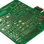
Multilayer Prototyping: Techniques That Speed Up a Build
A multilayer prototype is not simply a larger version of a two-layer build. It adds lamination cycles, registration tolerance and often impedance control, and each of those has to be planned before the order rather than discovered during it. This guide covers the techniques that make a multilayer prototyping run predictable.
What Makes Multilayer Prototyping Different
The extra cost is not only material. Each additional layer pair brings another lamination cycle, another registration step and another imaging step, and the process window narrows as the layer count rises. The prototype is also the first time the stackup is built, so any assumption in it is being tested for the first time.
That is why a multilayer prototype benefits more from preparation than a simple board does. The questions that a two-layer board answers implicitly, the multilayer board has to answer explicitly, and each unanswered question becomes a delay on the first build.
Choosing a Buildable Stackup
The stackup should be chosen for buildability as well as for electrical performance. A symmetric construction around the core resists warping during lamination, and standard core and prepreg thicknesses are more likely to be in stock. Both reduce the risk of a first-build surprise.
Where the electrical requirement allows a choice, a stackup that can be built on a standard process is worth more than one that is marginally thinner or marginally better electrically. Reviewing the layer stackup options with the fabricator before release is a few minutes of work that removes a week of risk.
<img src="https://www.gopcba.com/wp-content/uploads/2025/08/12温区氮气回流焊.jpg" alt="Multilayer prototyping stackup with lamination cycles and impedance coupon” />
Lamination Cycles and Blind Vias
Through-hole vias only require one lamination cycle, which is the reason they are the default. Blind and buried vias require sequential lamination, where layers are pressed, drilled and pressed again. Each additional cycle multiplies the registration risk and the process time.
That does not make them wrong, but it does mean they should be justified by the routing rather than adopted by default. Where a blind and buried via structure genuinely solves a routing or stub problem, it earns its cost; where it is used for convenience, it adds risk to the prototype without adding capability.
Documentation for a Multilayer Prototype
A multilayer prototype needs three documents that a two-layer board rarely does: a stackup drawing with material and thickness for each layer, an impedance requirement stating the target and the tolerance, and a finished thickness specification. Together they describe the board that the fabrication data alone cannot.
Material identification belongs in the same package. Naming the laminate class and the glass transition temperature rather than a specific product removes ambiguity without narrowing the source, and it lets the fabricator substitute an equivalent material if the first choice is not available.
<img src="https://www.gopcba.com/wp-content/uploads/2026/09/264-1.jpg" alt="Multilayer prototype panel with blind via structure and drill programme” />
Impedance Coupons and Verification
An impedance coupon is a strip of the same stackup included on the panel and measured to confirm the dielectric thickness and the trace geometry. It is the only practical way to verify a controlled impedance design without destroying a functional board, and its position should be planned at layout stage.
The coupon is also evidence. Where a customer or a regulator requires proof that the impedance is within tolerance, the measurement report from the coupon is that proof. Adding it after the panel has been laid out usually means placing it somewhere unrepresentative of the product area.
Prototype Quantity and Spares
Ordering a few extra boards costs very little once the tooling is paid for, and it protects the build from handling damage during assembly development. Recovering from a shortage costs a second tooling cycle and a second schedule, which is far more than the spares.
Spares are also useful for destructive checks. A microsection to confirm plating thickness, or a thermal cycle to check a via, consumes a board, and having one available prevents the test from being skipped.
Working With the Fabricator
The most productive conversation happens before the order. Confirming that the stackup is buildable, that the drill sizes are standard, and that the impedance targets are achievable on the material chosen removes the delays that otherwise appear after the data has been released.
A fabrication question raised at review costs a change to a document; the same question raised after the panel is made costs a new panel. Applying multilayer prototype requirements as a checklist turns that conversation into a routine step rather than a rescue.
Common Delays and How to Avoid Them
The first cause of delay is a missing stackup drawing, which forces the fabricator to infer dielectric thicknesses. The second is an impedance target that cannot be met on the chosen material without a narrower line than the process supports. The third is a drill size that is not standard for the aspect ratio being built.
All three are visible at review, and all three are resolved by a conversation rather than by a redesign. Building the check into the release process is what turns a multilayer prototype from an adventure into a scheduled step in the project.
Process Control and Verification
Reviewing the design before the data is released is far cheaper than correcting it after the panel is in the tank, because every step downstream inherits the decision made at the front end. Where a value sits close to a process limit, the drawing should say so, since the shop can then open the process window rather than working to a nominal figure that carries no tolerance.
The measurements that matter are the repeatable ones: conductor width and spacing, annular ring, finished hole size, plating thickness and surface finish are all verifiable on a coupon that travels with the panel. Documenting the assumption is part of the design work, and a short note on the drawing prevents a question that would otherwise arrive a day later and cost a day of schedule.
Where a value sits close to a process limit, the drawing should say so, since the shop can then open the process window rather than working to a nominal figure that carries no tolerance. Running a first article through the same checks as the production panel confirms that the two agree, and that comparison is the cheapest form of process control available at prototype stage.
Documenting the assumption is part of the design work, and a short note on the drawing prevents a question that would otherwise arrive a day later and cost a day of schedule. A stack-up that is drawn rather than described removes most of the ambiguity from a quotation, and it lets the fabricator price the board against the dielectric and copper weights that will actually be used.
FAQ
Do I need blind vias on a prototype? Only where the routing or the signal integrity genuinely requires them. They add a lamination cycle and registration risk, which is a real cost on a first build where the process itself is being proven.
Should the prototype stackup differ from production? No. The prototype exists to verify the production stackup, so changing it means the impedance, the thickness and the assembly behaviour remain unverified.
How many spare boards should I order? Enough to cover handling damage and one destructive check. On a prototype quantity the incremental cost is small compared with the cost of a second tooling cycle.