PCB Panelisation Design Rules for SMT Assembly Lines
A bare board cannot be assembled by itself. It needs a frame that the conveyor can grip, holes the machine can locate, and a way to separate the finished product without cracking it. Panelisation is the art of arranging circuits on a carrier so that all of those needs are met at once, and it is one of the few layout decisions that directly changes assembly cost.
Why Panelisation Drives Assembly Efficiency
Assembly equipment handles panels, not individual boards, and every machine has a minimum and maximum size it can accept. Packing more circuits onto one carrier raises throughput and reduces handling, but it also increases the risk that a single defect destroys several good units. The right balance depends on volume, board size, and how the product will be separated.
Panelisation also determines how much material is wasted. Rails and tabs consume laminate that never becomes product, and an inefficient array can add several percent to material cost on a large program. Reviewing the layout before the panel drawing is finalised is far cheaper than rerunning the artwork after the stencil has been ordered.
Panel Size Limits and Machine Constraints
Each machine in the line has a usable size window: the printer, the placement platforms, the reflow oven, and the inspection systems all differ. A panel that fits the printer may exceed the conveyor width of the placement machine or hang outside the heated zone of the oven. The array must satisfy the narrowest constraint in the whole line.
Thickness and rigidity matter as much as length and width. A large panel made from thin laminate sags under its own weight, so its size may be limited by flatness rather than by machine dimensions. Where the product is inherently thin, splitting the array into smaller panels often costs less than adding support tooling to keep a large one flat.
Rails, Tooling Strips and Edge Clearance
Rails are the strips along the edges that the conveyor grips. Their width is chosen to suit the machine edge hold, and the area within them must be free of components and vias that could be damaged. Where the product fills the panel edge to edge, a rail is still required, and it consumes material that must be accounted for in the quotation.
Some lines prefer tooling strips with tooling holes rather than wide rails, especially when the panel is expensive. In that case the strip needs enough width to accommodate the holes and the registration tolerance without deforming. Whichever format is used, keep the edge zone free of solder mask features that could confuse edge sensors.

Breakaway Tabs and Router Paths
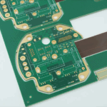
Breakaway tabs connect the product to the rails and are removed after assembly. Their number, width, and position control how much stress reaches the board during separation. Tabs placed near a corner or beside a heavy component concentrate that stress in the worst possible place, so they are normally distributed along the edges instead.
Router paths need clearance for the bit diameter, and the cut should not pass closer to a trace than the mechanical tolerance allows. V-scoring is an alternative for straight edges, but it leaves a visible scored line and cannot follow a curve. Choose the separation method before finalising the outline, because each one imposes its own keep-out.
Fiducial and Tooling Hole Placement
Fiducials give the placement machine a reference, and they must be placed where vision can see them on every panel. Global fiducials usually sit diagonally across the array, with local fiducials near fine-pitch parts. They need clear contrast, a defined mask opening, and a keep-out zone free of traces and silkscreen that could confuse the pattern.
Tooling holes serve the printer, the placement machine, and often the test fixture. They should be positioned from the same datum as the circuits, sized to a standard pin, and placed away from tabs that may distort during routing. Two holes are normally enough; a third can over-constrain the panel when tolerances differ across the stack.
<img src="https://www.gopcba.com/wp-content/uploads/2026/08/PCB-Fabrication-Process.jpg.webp" alt="Router depanelling a PCB panel along tabs next to the rail” />
Component-to-Edge and Keep-Out Rules
Components need clearance from the panel edge for two reasons. The conveyor and the machine nozzles must not collide with them, and depanelling stress must not reach their solder joints. Tall parts such as connectors and electrolytic capacitors deserve more clearance than a chip resistor, because they present a longer lever arm during handling.
Keep-out also applies to vias, test points, and anything that the separation method could damage. Define these distances in the fabrication notes so that the fabricator does not have to interpret a marginal layout. A few tenths of a millimetre borrowed from a keep-out is rarely worth a cracked joint discovered after functional test.
Panel Bow, Twist and Copper Balance
Copper distribution affects how a panel behaves through lamination, reflow, and cooling. A dense area next to an empty one sets up a gradient that shows as bow or twist, and a warped panel misprints, misplaces, and jams conveyors. Balancing copper across the array is part of the panelisation task, not an afterthought for the fabricator.
Thieving and dummy pads help equalise the metal, and symmetrical stackups reduce the tendency to twist. Where the product itself is inherently unbalanced, orienting the circuits so that heavy areas alternate can improve the result. Measuring flatness after assembly, not only after fabrication, confirms whether the approach worked.
Depanelling Methods and Mechanical Stress
Routing, V-scoring, laser cutting, and punching all impose different loads. Routing is flexible and leaves a clean edge, but the bit applies a side load that a thin board can feel. V-scoring is fast for straight edges yet transmits bending stress along the whole line when the boards are snapped apart. Lasers avoid mechanical load but cost more per cut.
Support during separation is as important as the method. Backing the product near the cut, pivoting the waste material away, and avoiding a rigid clamp reduces the chance of a cracked microvia or a lifted pad. Because depanelling occurs after most of the value has been added, a damaged board at this stage is the most expensive defect in the process.
Review Checklist Before Release
Before the panel drawing is released, confirm that the array fits every machine in the line, that rails and tooling strips meet the machine’s edge requirements, and that fiducials and tooling holes sit on the same datum as the circuits. Check component-to-edge clearance, tab placement relative to heavy parts, and the keep-outs demanded by the separation method.
Then review copper balance, panel thickness, and expected flatness. Compare the panel against previous products that ran well and note any deviation. Finally, confirm the material utilisation and the resulting cost per board, since an array that is only marginally more efficient than a simpler one is rarely worth the added risk.
FAQ
How wide should rails be? The width is set by the conveyor and the edge hold of the machines in the line, typically 3 to 8 millimetres, plus whatever the tooling holes and tabs require. Ask the assembly house for its preferred value rather than designing to a generic figure, because the requirement is machine specific.
How many breakaway tabs does a board need? Enough to hold the product rigidly during assembly without concentrating stress at a sensitive location. Two to four tabs per side is common for small boards, with more for heavier products. Tabs next to heavy components should be avoided, since they transmit the separation load directly into the joints.
Is V-scoring better than routing? V-scoring is faster and cheaper for straight, full-length edges and leaves minimal burrs, but it transmits bending stress across the whole panel during snapping and cannot follow a curve. Routing is more flexible and gentler on complex outlines, at the cost of cycle time and bit wear.