Finding EMC Weak Points Before the Compliance Test
Most products fail an immunity test in a specific place, at a specific frequency, and for a reason that is not visible on the schematic. The failure is usually the consequence of one small structure: a trace that acts as an antenna, a connector whose shield bond is inductive, a reset line that runs beside a switching node. Finding that structure before the formal test turns an expensive iterative process into a short engineering exercise.
The method is to apply a controlled field locally rather than to illuminate the whole product and wait for a failure. A small field source placed close to a circuit injects a disturbance into one area at a time, and the reaction of the equipment identifies the sensitive region. This is more informative than a system level test at a distance, because the source of the failure is immediately adjacent to the part of the design that reacted to it.
Locating the Sensitive Area
The process begins with a coarse source that excites a broad area. The equipment is operated in the state where it is most vulnerable, and any deviation from normal behaviour is recorded along with the position of the source. A low resolution probe covers a large region quickly, so the first pass identifies the board, the connector or the cable that responds, without yet identifying the exact component responsible.
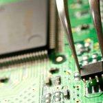
A high resolution source is then used to focus the field on a smaller area, and the search is repeated until the sensitive structure is located precisely. This second stage is what makes the technique useful: knowing that a board fails tells the engineer nothing actionable, while knowing that a particular trace beside a particular connector fails tells them exactly what to change. The finer probe may also expose sub-critical weaknesses that a full-scale test never reaches, which are worth removing even though they do not currently cause a failure.
<img src="https://www.gopcba.com/wp-content/uploads/2026/06/DWDM波分复用设备-PCBA.jpg" alt="Field probe positioned over a circuit board during immunity testing” />
From Broad Excitation to a Specific Point
The distinction between the two stages matters for another reason. A product can pass a standard test while containing a structure that is only marginally stable, and that structure will fail when the production variation, the cable routing or the operating state changes. Applying a local field with enough intensity to reveal the margin, rather than only enough to reproduce the compliance condition, exposes the weakness while it is still cheap to fix.
The same idea applies in reverse when the problem is emission rather than immunity. A near field scan of the board while it operates identifies the structures that radiate, and the location of the strongest field usually corresponds to the loop or the trace that needs attention. Emission and immunity are often two views of the same geometry, so a structure identified by one method is worth examining with the other.
What Counts as a Failure
The investigation is only as good as the definition of failure. A product can react to a disturbance without appearing to malfunction, so the criterion has to be stated in measurable terms before the search begins. Typical definitions include a bit error on a communication link, a reset or a brown-out event, a change in an analogue reading beyond a specified tolerance, or a corrupted sample in a data stream. Vague indications such as an audible change or an unexplained display artefact are not useful because they cannot be repeated.
Once the criterion is defined, the equipment should be operated in the state where it is most vulnerable. A processor idling at low speed produces a different EMC weak points profile from the same processor running at full load with its communication interfaces active, and the worst case is often a specific combination of operating mode and interface traffic rather than the average condition. Repeating the search in each relevant mode is part of the technique, not an optional refinement.
Fixing What You Find
The remedy depends on the mechanism the probe has exposed, and the location usually makes the mechanism obvious. A sensitive input that reacts when the probe approaches its trace is picking up a field inductively, and the fix is to shorten the loop or route the trace closer to its reference plane. A circuit that reacts when the probe approaches a connector suggests that the shield bond or the connector grounding is the weak point, which is addressed at the mechanical interface.
A device that reacts when the probe approaches its supply pins is responding to a disturbance that reaches it through the power distribution network, which points at decoupling and plane impedance rather than at signal routing. Recognising these patterns is what turns immunity testing from a search into a diagnosis, and the measures themselves follow from the general practice of EMI suppression and the small signal layout conventions in mixed signal design guidelines.
Building It Into the Project
The technique is most valuable when it is applied early rather than as a rectification exercise. Applying a local field during the first prototype build, with the equipment in its intended enclosure, identifies the weak points while a layout change still costs an afternoon. Waiting until the formal immunity test means the options are limited to adding material, and the result is a product with less design margin than it could have had.
The results should be recorded as part of the design file: the frequency and intensity at which each area reacted, the definition of failure used, and the change made in response. That record makes the next revision comparable, and it demonstrates the margin obtained rather than merely the absence of a failure. The measurement discipline that supports this is the same as that described in PCB design quality characteristics, and the interface practices that most often prevent immunity problems are covered in the rules for ESD on board edges.
Choosing the Probe for the Task
Two characteristics define a field probe for this work: the size of the field it produces at its tip and the resolution of that field. A coarse probe with a large excitation area is used for the initial sweep, because it covers a board quickly and identifies the region that responds. A fine probe concentrates the same disturbance into a small volume, which is what allows a specific trace or package pin to be identified without exciting its neighbours at the same time.
The frequency content of the field also has to be selected. A probe driven at a single frequency is useful for characterising a known problem, while a broadband excitation reveals responses across a range. In practice the search starts broadband to find where the equipment is sensitive, then narrows to the specific frequency at which the response occurs so that the mechanism can be related to a known clock, a switching frequency or a resonance in the layout.
FAQ
Is a local field probe a substitute for the compliance test? No. It is a diagnostic tool that locates weaknesses early. Compliance is still demonstrated by the standard test on the final product.
What intensity should be used? Enough to reveal margin rather than only enough to reproduce the compliance condition. The goal is to find the structures that are close to failing, not only those that already fail.
Why is a sub-critical weakness worth fixing? Because production variation, cable routing and operating conditions will change, and a structure that passes today may not pass in a different configuration or after a component substitution.