PCB Structural Design: Board Size, Placement and Thermal
Structural design is the part of the layout that is settled before routing begins: how large the board is, how the components are arranged on it, how the supply is decoupled and how heat leaves the assembly. These decisions constrain everything that follows, and correcting them later means moving components rather than editing traces.
Choosing the Board Size
Board size is a compromise rather than a preference. A larger board allows shorter interconnection between functional blocks and lower routing density, but it lengthens the traces between distant parts, raises the impedance and cost, and makes the assembly more susceptible to mechanical flexing.
A smaller board reduces cost and improves thermal coupling to the enclosure, but concentrates the heat and makes the routing denser. The right size is the smallest that still allows the routing to be completed with reasonable spacing and the heat to leave each device.
Component Placement by Function
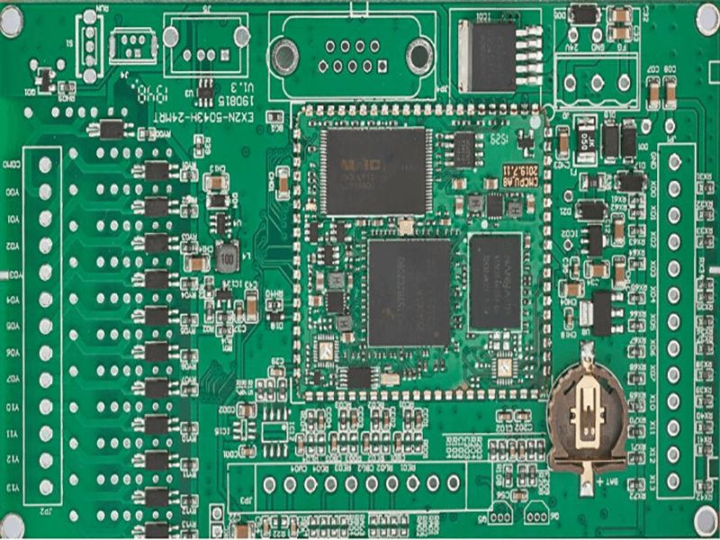
Components that work together belong together. A clock generator, its oscillator and the clock input of the processor should sit in the same small area, because a clock distributed across the board picks up noise and radiates it into everything it passes.
Noisy and sensitive circuits should be separated rather than interleaved. Where the separation is not possible on one board, a grounded guard band between the two regions is the next best option, and in extreme cases the two functions belong on different boards entirely.

Decoupling Configuration
The supply network is built in layers. A bulk electrolytic capacitor of ten to one hundred microfarads at the point where the supply enters the board absorbs slow variations, while a small ceramic capacitor at each integrated circuit handles the fast current demand when the device switches.
Where space prevents a capacitor at every device, a shared tantalum capacitor of a few microfarads can serve a group of four to ten chips, because its impedance at high frequency is low. The essential point is that the capacitor belongs close to the load, with short leads, since a long connection negates the benefit.
Thermal Design
Heat leaves a board by convection and conduction, and the arrangement of components determines how easily it does so. Where the assembly is mounted vertically and the boards are spaced by at least a couple of centimetres, natural convection is more effective than in a horizontal stack.
Devices should be grouped by dissipation and by sensitivity. Components that tolerate heat go downstream in the airflow, and temperature-sensitive parts go where the air is coolest rather than directly above a power device. Large dissipation near the board edge shortens the path to the enclosure.
Airflow and Enclosure Interaction
Air follows the path of least resistance, so a board with a large empty region and a dense region will see most of the flow in the empty area. Spreading the components evenly, and avoiding walls of tall parts that block the channel, is what makes cooling predictable.
The enclosure is part of the thermal design. A board that relies on airflow needs vents, and one that conducts heat into a metal chassis needs a defined thermal path to it, which is a mechanical requirement as much as an electrical one.
Electromagnetic Compatibility
Compatibility starts with geometry. Narrow traces carrying fast edges have more inductance and radiate more, so trace width is an EMC parameter as well as a current one, and a return path immediately beneath each signal contains the field that would otherwise spread.
Connectors and cables are the other major contributor. A cable acts as an antenna, and the current that drives it passes through the board, so filtering at the connector and a solid ground reference at the interface reduce emissions far more effectively than changes elsewhere.
Structural and Mechanical Constraints
The outline, mounting points and the position of connectors come from the enclosure, and they should be fixed before placement rather than adjusted afterwards. A board that fits the electronics but not the housing is not finished.
Support matters as well. A large board that is only fixed at two corners will flex during assembly and in service, and the flexing loads solder joints on heavy components. Additional mounting points, or a stiffener along the weak axis, remove that failure mode. The outline and mounting definition should therefore be part of the electrical layout rather than a later mechanical task.
Signal Integrity in the Structure
The same arrangement governs how signals behave. A reference plane under a routing layer gives every trace a defined impedance, and grouping buses together with consistent spacing keeps their behaviour predictable.
Where the design mixes analogue and digital functions, the structure has to keep their return currents apart. That is a placement and partitioning question rather than a routing one, and it is addressed in the general guidance for mixed-signal boards.
Reviewing the Structure
The structural decisions should be reviewed before routing starts, because that is the point at which they are still cheap to change. Confirm the board size against the enclosure, the placement against the signal flow, the decoupling against the supply pins and the thermal path against the airflow.
Then confirm that the design rules that will be used for routing reflect those decisions, as described in manufacturable design practice. A structure that is correct but not reflected in the rule set will be undone by the router.
Layer Structure and Stackup
The stackup follows the structure. A design that needs a continuous reference for every routing layer needs at least one plane per pair of signal layers, and the number of supply rails determines how many of those planes can be dedicated to power rather than ground.
The stackup should also be symmetrical, so that the board stays flat through lamination and reflow. An asymmetric construction may look acceptable on the drawing and bow during assembly, which then affects placement accuracy on the second side.
Design for Manufacture
The structure should be buildable at the fabricator’s normal capability rather than at its limit. Minimum trace and spacing, the smallest drill, the annular ring and the clearance from copper to the board edge all influence yield, and a structure that works at the limit will cost more and arrive later.
Assembly imposes its own constraints: fiducials for the placement machine, adequate spacing for the stencil and a component orientation that suits the reflow profile. Building those requirements into the placement is easier than adding them later.
Documenting the Structure
A short document recording the outline, the mounting arrangement, the placement zones and the thermal assumptions makes the layout reviewable by someone who was not involved in the decisions. It also makes a later revision far quicker.
The document should include what was deliberately excluded, such as a function deliberately placed away from a noisy area, since a future engineer with no record of the reason is likely to move it back and reintroduce the problem.
FAQ
Does a smaller board always reduce cost? It reduces material and often the fabrication price, but it concentrates heat and increases routing density, which can cost more in assembly and in reliability than it saves.
How close should a decoupling capacitor be? As close as the layout permits, ideally within a few millimetres of the supply pin it serves. Distance adds inductance that cancels the benefit of the capacitor.
How far apart should boards be in a rack? At least two centimetres between vertical boards is a common starting point for natural convection. Forced airflow changes the requirement.