Castellation: Preparation, Placement and Process Control
A castellation is a plated half hole cut into the edge of a board so that the module can be soldered onto a carrier like a surface mount component, and it is the standard way to build a small sub assembly that has to be tested before it is committed to a product. The feature looks simple, but it combines drilling, plating and routing tolerances in a way that leaves very little margin for error. Those three operations happen at different stages, so a mistake in any one of them only becomes visible at the very end.
What a Castellation Is
The hole is drilled and plated like any other through hole, and then the board outline is routed through the centre of it so that half of the barrel remains on the finished edge. The exposed copper fills with solder when the module is placed and reflowed, forming a joint that is visible from the side.
That visibility is one of the main attractions. Unlike a ball grid array, the joint can be inspected with ordinary optical equipment, and a rework operation on a single connection is practical rather than a specialist task.
How the Holes Are Formed
The holes are drilled before plating, so the barrel is a full cylindrical deposit at that stage. The board is then routed along the outline, and the position of the cut relative to the hole centre decides how much of the barrel survives and how symmetric the finished feature is.
A cut that misses the centre leaves a deeper or shallower half hole, and the variation appears in the solder volume rather than in the appearance of the pad. Small modules typically use holes from half a millimetre to a millimetre in diameter, and the tolerance on the cut position is what limits the achievable consistency. That tolerance is normally tighter than the general outline tolerance, because the solder volume depends on it directly.
Plating the Half Hole
Because the cut happens after plating, the copper on the cut face is a cross section of the barrel rather than a plated surface. That exposes the copper to oxidation and to the environment, and it means the wettable area at the cut face depends on how well the barrel was plated in the first place.
The plating therefore has to be sound all the way through the hole, with no thin patches or voids. Where the deposit is marginal, the half hole presents a mixed surface of copper and laminate, and the solder does not wet it evenly. Our hole copper notes describe the barrel that has to survive the cut. Plating thickness in the barrel is therefore specified rather than assumed, and a coupon section is the evidence that the figure was achieved.
Pad Geometry and Solder Fillet
The pad on the module and the land on the carrier both have to allow for the castellation and for the solder fillet that will form around it. Typically the pad is a circle that overlaps the hole, and the land on the carrier extends slightly beyond it so that a fillet can form on three sides.
The solder fillet is the visible evidence that the joint is sound, and its shape is what the acceptance criteria describe. A joint with no fillet has insufficient solder, while a very large one suggests that the paste volume is too generous and that bridging between adjacent castellations is likely. Our land pattern notes describe the geometry. A stencil aperture sized to the land rather than to the castellation keeps the paste where the fillet needs it.
Board Edge Clearance and Outline Routing
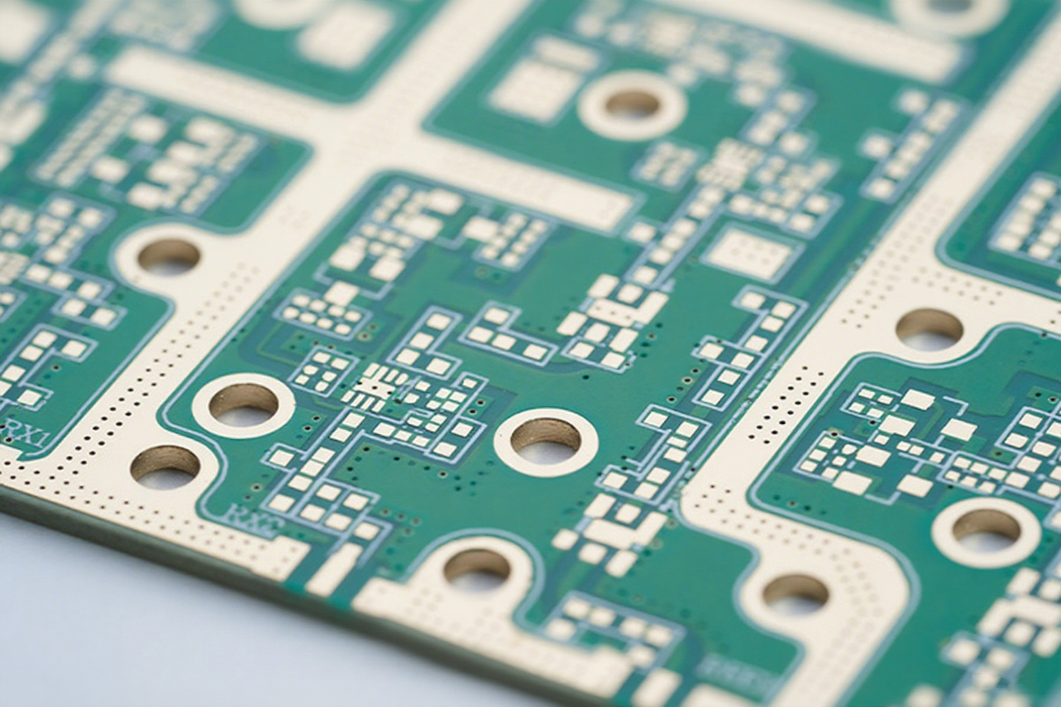
The outline has to be routed rather than scored, because scoring cannot follow a contour or produce the clean edge a castellation needs. The router bit diameter sets the minimum internal radius of the outline and the space required between features at the board edge.
Clearance also has to be allowed for the bit path relative to any copper that is not meant to be exposed. A cut that strays into a trace damages the module permanently, so the copper keep out around the castellation is wider than the pad geometry alone would suggest. Our board outline notes cover the tolerance side. Where the module outline is complex, the routing programme is often the longest single item in the fabrication lead time.
Module Assembly and Reflow
The module is placed like a component and reflowed with the rest of the assembly, which means it has to survive the same thermal profile. Its own internal joints must also survive, so a module that was assembled with a low melting solder cannot be processed with a high temperature lead free profile.
Placement accuracy matters because the castellations on the module and the lands on the carrier are small. A misplacement of a fraction of a millimetre moves the solder volume to one side of the joint and leaves the other side unfilleted, which is exactly the defect that a visual inspection will find.
Inspection and Acceptance
Inspection is visual and from the side, which is the advantage of the design. The criteria should describe the fillet profile on the pad and on the castellation, the maximum acceptable void, and the bridging limit between adjacent joints.
Where the module has a high castellation count, the joints at the ends of the row are the ones to check first, because those are the positions where the placement error and the thermal gradient are largest. Our fabrication notes checklist lists the items worth recording for each lot. A photograph of an accepted joint, kept at the bench, is a useful reference for a new operator.
Reliability and Thermal Cycling
A castellated joint is a fillet joint rather than a ball joint, so it behaves more like a leaded connection than like a BGA. It tolerates thermal cycling well when there is enough solder and a proper fillet, and it fails early when the solder volume is marginal.
The module substrate and the carrier also expand at different rates, and the joint has to absorb that difference. Where a large module is used, the castellations at the outer corners carry the highest strain, which is why the joint there deserves the most attention during qualification.
Specifying Castellations on the Drawing
The drawing should give the hole diameter, the cut position relative to the hole centre, the pad diameter and the plating thickness, together with a note that the outline is to be routed rather than scored. It should also say whether the cut face is to be inspected for exposed laminate.
Where several castellations are used in a row, the pitch and the tolerance on the row position matter as much as the individual features. Getting both onto the drawing before the panel is built is the cheapest way to avoid a module that assembles badly for reasons nobody can quite identify. Where the module is purchased rather than built in house, the same information has to be requested from the supplier instead of assumed.
FAQ
Can castellations be added to an existing design? They can, provided the hole spacing and the keep out allow it. The change usually means re-drilling and re-routing the panel, so it is normally treated as a new revision rather than an adjustment.
Is a castellated module always more expensive? The drilling and routing add cost, and the half hole reduces the yield at the edge of the route. Against that, the assembly and inspection savings are often larger, particularly on small modules.
How does gopcb build castellated modules? We control the hole position and the cut position to the agreed tolerance, verify the barrel by section, route the outline on a dedicated programme, and inspect the finished castellations for plating coverage and edge quality.