Smartphone PCB Design Feasibility and Routing Planning
A handset board packs several radios, a display, cameras and a battery into a space smaller than a card. Smartphone pcb design is a planning problem before it is a drawing problem, because the routing capacity has to be proven before the layout starts.
Why Early Evaluation Matters
The board area available in a phone is decided by the battery, the display and the cameras before the electronics are considered. The remaining space has to carry every component and every connection.
With a target of complete routing, and with signal quality and manufacturability constraints on top, the feasibility of a proposed arrangement is not obvious. It has to be evaluated rather than estimated by experience alone.
Feasibility Analysis
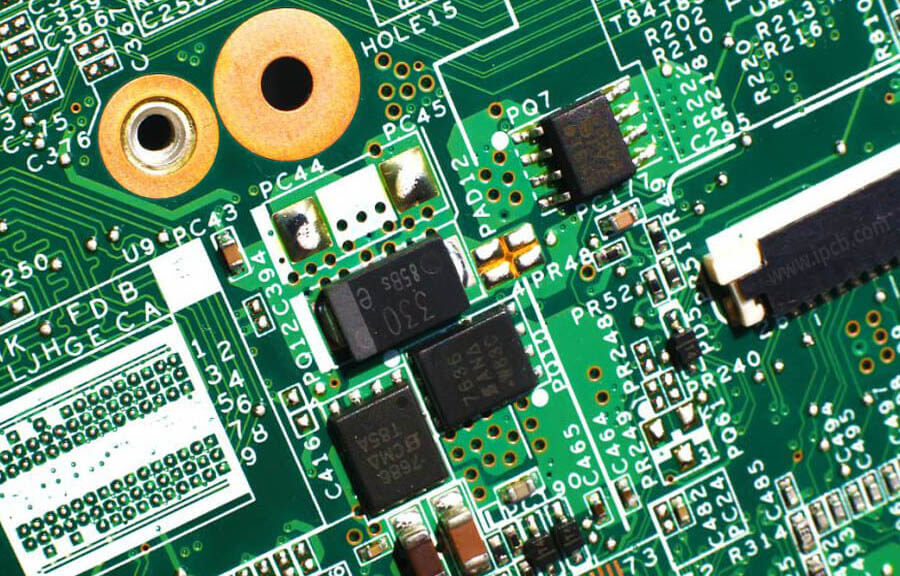
The feasibility study answers two questions: whether the components fit, and whether the connections between them can be routed. Both are answered at a coarse level, using estimated channel widths rather than detailed geometry.
The study is repeated for each candidate platform, because the same product is often evaluated with two or three different chipset arrangements. The comparison is what allows the platform decision to be made on evidence.
Routing Channels
A routing channel is the space between two rows of pins or two component areas that is available for the connections crossing it. Its width, divided by the trace and space, gives the number of signals it can carry.
Counting the connections that must cross each channel, and comparing that with the capacity, shows where the design is short. The result is also a specification for the layer count and the via technology.

Estimating the Routing Capacity
The estimate uses the pin pitch, the trace width, the clearance and the number of layers available for routing. It is deliberately approximate, because it is used to compare options rather than to produce artwork.
Where the estimate shows a shortfall, the response is to change the arrangement, add a layer or adopt finer geometry. Changing the arrangement is almost always the cheapest of the three.
Design Reuse From a Platform
Most handset boards are derived from a platform reference design supplied with the chipset. Reusing it means that the memory, the power and the radio sections are already validated.
Reuse is what makes a short development cycle possible. The parts that change are the mechanical outline, the connector positions and the user interface, and those are the parts that need the evaluation.
Signal Quality Constraints
The high speed interfaces, the memory bus, the display link and the camera links each have a length and impedance requirement. The radio path has a loss and isolation requirement.
Those requirements reduce the routing capacity, because a channel that carries a differential pair can hold fewer signals than one that carries single ended lines. The budget has to be kept for them during planning rather than discovered during routing.
Manufacturability Constraints
Fine geometry has a cost and a yield implication. The smallest via, the thinnest dielectric and the finest line all have to be within the capability of the shop that will build the board.
The evaluation therefore includes the process window. A design that fits only at the absolute limit of the process is a design that will be expensive and slow to produce, as described in our notes on manufacturability.
Board Outline and Component Density
The outline comes from the mechanical design, and the components are placed inside it. Component density is highest around the processor, where the memory and the power devices cluster.
That area sets the layer count and the via technology for the whole board. The evaluation focuses there, because the rest of the board is easier by comparison.
Rigid and Flexible Sections
Some handsets use a rigid board with a flexible tail for the display or the buttons. The transition between the two has its own design rules, including bend radius and stiffener placement.
The flexible section is treated as a separate design object with its own stackup. Its impedance and its bend requirements are specified together with the connectors at each end.
Thermal Limits in a Sealed Handset
A phone has no fan and very little surface, so the heat from the processor and the power amplifier has to spread across the whole board and the case. Copper area is the design lever.
The thermal limit is often what sets the sustained performance of the product. The evaluation should include an estimate of the board temperature at the worst case load, because that figure affects the processor choice.
The Evaluation Data as a Design Record
The channel counts, the layer estimate and the assumptions behind them are worth keeping. When the layout later runs short of space, the record shows whether the assumption was wrong or the design has changed.
Keeping the evaluation with the released design also shortens the next project, because the platform data can be reused. The practice is the same as the design quality record used for any board.
Team Collaboration
The evaluation involves the mechanical, the electrical and the manufacturing teams, and it is most useful when it happens before the layout starts. A study produced after the fact is a description rather than a decision.
Sharing one model of the board keeps the three views consistent. The mechanical envelope, the placement and the routing estimate have to describe the same physical object.
Revision Planning
A handset board usually goes through several revisions before production, and each of them costs tooling and time. Planning the revisions in advance, with the objectives of each one stated, keeps the count down.
The channels that are close to their capacity are the ones most likely to force a change, so they are watched from the first build. The same discipline applies to any dense board, as described in our design and fabrication notes.
Working With the Chipset Vendor
The platform documentation, the reference layout and the design review carried out by the vendor together reduce the risk in the sections that are hardest to test. Access to that support is part of the platform choice.
Vendor reviews are most useful when they happen at the feasibility stage rather than at the end. A question about an interface arrangement is cheap before the layout and expensive afterwards.
Prototype Builds and Their Purpose
The first build of a dense board is a test of the plan rather than of the product. Its purpose is to confirm the placement, the escape and the routing channels while a change is still affordable.
Each subsequent build should have a stated objective, so that the number of builds stays under control. The discipline used here is the same as in any PCBA development programme.
FAQ
Why is a feasibility study needed when the design is reused? Because the outline, the connectors and the user interface change in every product, and those changes move the routing channels.
How accurate is the channel estimate? It is approximate by design. Its value is in comparing options and in showing a shortfall early, not in predicting the exact number of traces.
What usually limits the number of layers? The escape from the processor and the memory bus. Those two areas decide the layer count for the whole board.