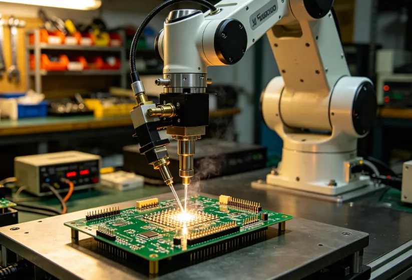
Board Coplanarity For Connector Mounting
Coplanarity is the property of a set of features lying in the same plane. For a fine pitch connector it describes how closely the solder tails or the pads of the connector lie in one plane relative to the board surface, and it decides whether every joint in the row can form at the same time during reflow.
This article explains why coplanarity matters, how it is measured, how board warp and paste volume interact with it, and how the assembly is specified.
Why It Decides Whether The Joints Form
In a reflow process the connector sits on a deposit of paste, and every tail has to touch its deposit. The tails of a connector are held in a plastic body that is rigid, so the tails lie in a plane defined by the body. The board surface underneath is not necessarily in the same plane, because the board warps. Where the gap between a tail and its pad exceeds the height of the paste deposit, that joint does not form at all, and the result is an open circuit that is visible only if the joint is inspected.
The tolerance is small. A paste deposit a tenth of a millimetre thick has to bridge the sum of the board warp, the connector’s own coplanarity and the placement error. On a fine pitch connector with hundreds of tails across a long body, the specification for both the component and the board is a fraction of that figure, which is why this is one of the few places where board flatness is specified as a requirement rather than assumed. What happens to the deposit during placement is described under placement order and pad positioning.
Measuring And Specifying Coplanarity
The measurement is made by placing the connector or the board on a reference surface and measuring the deviation of each tail or pad from that surface. For a connector, the specification usually gives a maximum deviation across the whole row and a maximum for any single tail. For a board, the equivalent figure is the flatness of the surface in the region where the connector will sit, and it is measured on the bare board before assembly.
The measurement is affected by how the part is supported. A board measured on a flat granite plate reflects its natural shape, whereas the same board clamped in a fixture during assembly is forced into the shape of the fixture. That is why the specification is normally written for the supported condition: the relevant question is not how flat the board is in free air, but how flat it is when it is held on the conveyor and pressed by the placement nozzle. The warp that the laminate develops during processing is described under PCB dimensional stability and expansion.

Board Warp And How It Is Controlled
Board warp comes from the stack and from the copper distribution. A stack with an asymmetric arrangement of layers, or with a heavy plane on one side and a sparse layer on the other, will curl during lamination and again during reflow. The control is to make the stack symmetrical and to balance the copper, both of which are decisions taken before the artwork is released. Where a connector footprint sits in an area of the board that is far from symmetrical in copper, the local warp is worse than the board average.
Assembly adds its own contribution. A board that supports a heavy connector and is held only at its edges will sag, and the sag changes the effective coplanarity during reflow, which is the moment that matters. Support under the connector footprint, provided by a pallet or a tooling pin, removes most of that contribution and is frequently the difference between a process that works and one that does not. The mechanical arrangements that support the board during assembly belong with the general fixing design covered under board outline and mounting design.
Paste Volume And Deposit Shape
The deposit is the layer that absorbs the errors, so its volume and its height are process parameters that can be used to compensate. A deposit that is slightly thicker bridges a larger gap, at the cost of more solder in the joint and therefore more risk of bridging between adjacent tails. A deposit that is too thin cannot reach a tail that is standing off the pad, and the joint remains open.
The shape of the deposit matters as much as its volume. A deposit that has slumped, or that is printed with a ragged edge, does not present a uniform surface to the tail, so the contact depends on where the tail lands. The stencil, the aperture and the print parameters together set the shape, and the design of the aperture follows the same rules as any other fine pitch footprint. The relation between the deposit and the pad it sits on is treated under design guidelines for manufacturability.
Verifying The Assembly
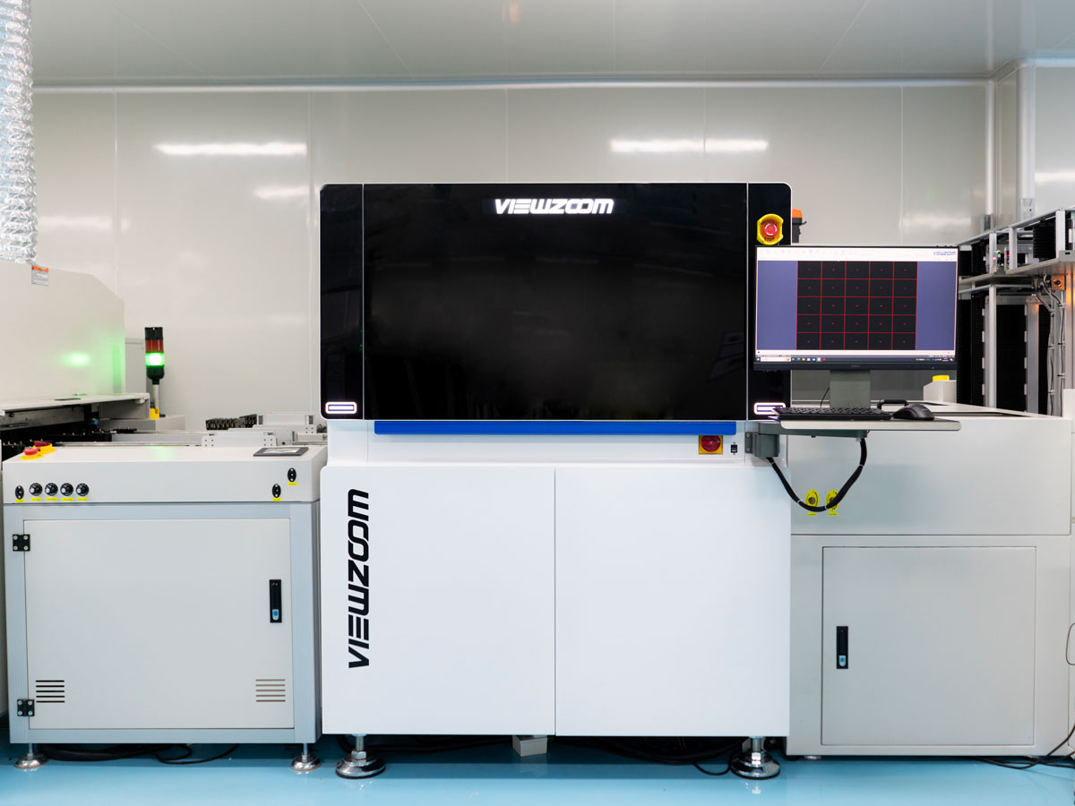
The verification of a coplanarity-sensitive assembly is done by inspecting the joints, not by measuring the parts. Automated optical inspection sees the tail and the fillet from the side, and it can detect a tail that is standing clear of the pad. X-ray sees the joint from above and detects a void or a missing fillet, though it is less able to see a joint that has formed only at one side.
Where the assembly is critical, a sample is sectioned to show the joint at the two ends of the row and at the middle, which are the positions where the gaps are largest. A pull test on a sample connector gives a quantitative measure of the weakest joint. All three checks are worth doing on the first article, and one of them is normally retained as a periodic check afterwards.
Design And Process Measures
The design measures are to keep the stack symmetrical, to keep the copper balanced under the connector, and to place the connector where the board is flattest rather than where it is convenient. Where a large connector must sit in a region of unbalanced copper, adding thieving to the opposite side of the board reduces the local disparity. The supporting structure for the connector, and any stiffener that holds the board flat beneath it, is part of the mechanical design of the assembly.
The process measures are to support the board directly under the connector footprint, to place the connector early in the sequence so that the board has not been heated repeatedly, and to verify the paste deposit volume on the pads of that footprint specifically rather than on the board as a whole. Together these measures turn a coplanarity requirement from a specification that the assembly is measured against into a condition that the process maintains.
FAQ
Is coplanarity a component specification or a board specification? It is both, and the two add together. The connector has a coplanarity figure, the board has a flatness figure in the same region, and the paste deposit has to bridge the sum of the two plus the placement error.
Does a thicker stencil solve a coplanarity problem? It can mask the symptom by providing more paste to bridge the gap, at the cost of more solder in each joint and a higher risk of bridging between adjacent tails. It is a compensation, not a cure.
Why does the problem appear only on the outer tails? The ends of a long connector body are where the accumulated deviation is largest, and they are also the positions least well supported by the board if it is held only at its edges. Supporting the board under the footprint addresses both.