
Coverlay Adhesive Selection For Flex Circuits
A coverlay is the flexible equivalent of a solder mask. It is a layer of polyimide film coated with an adhesive that is laminated over the finished circuit to protect the conductors and to define the areas where components or connectors will be attached. It is a structural layer rather than a printed coating, and it changes the mechanical behaviour of the circuit.
It is chosen for mechanical reasons rather than for appearance. The coverlay has to survive bending, it must not crack at a tight bend radius, and its adhesive must stay bonded through soldering and through the thermal cycles of the application. Those three requirements decide the film and the adhesive between them.
What A Coverlay Does
The coverlay protects the conductors from handling, from moisture and from accidental contact, and it provides the dielectric layer that separates the circuit from anything pressed against it. It also defines the flexing behaviour, since the film thickness and the adhesive together set how far the assembly can bend without damage.
In a dynamic flex application the coverlay is part of the mechanical design. The neutral axis of the bend lies between the copper and the coverlay, so the film thickness and the copper thickness both influence how much strain the copper sees at a given bend radius.
Acrylic Versus Epoxy Adhesive
An acrylic adhesive is the traditional choice because it stays flexible at low temperature, tolerates repeated bending and is forgiving during lamination. Its limitation is temperature: standard acrylic softens above roughly 120 C, which is close to the temperatures seen in a lead free reflow process.
Epoxy based adhesives offer better high temperature performance and lower moisture absorption, at the cost of a stiffer bond and a narrower lamination window. The choice should follow the assembly process, so a board that will go through lead free reflow needs an adhesive rated for it. The wider material picture is described under PCB dimensional stability and expansion.
Lamination Of The Coverlay
Lamination is done in a press with controlled temperature, pressure and time, usually with a release film and a compliant pad to distribute the pressure evenly. The adhesive must flow enough to fill the gaps between conductors without squeezing out so far that the bond line becomes too thin in the open areas.
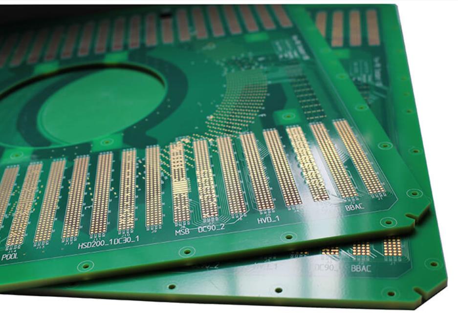
The process window is defined by the adhesive supplier and should be verified on each batch. Too little flow leaves voids over the conductors; too much flow starves the bond line and produces a weak area that delaminates later. A test coupon with a representative track pattern is the best way to confirm the window.
Bend Radius And Adhesive Thickness
Bend radius is the parameter that governs coverlay selection more than any other. A thin coverlay follows a tight radius without cracking, while a thick one resists bending and puts more strain on the copper. For a static bend, a radius of ten times the total thickness is a common starting rule; for a dynamic bend the ratio has to be much larger.
Adhesive thickness also matters, because the adhesive is the compliant layer that absorbs strain. A very thin bond line transfers the strain directly into the coverlay film and can cause the film to craze, while a thick one cushions the copper but adds height and reduces the resolution of the openings.
Opening The Coverlay For Pads
Openings for pads and connectors are made by punching, laser cutting or photolithography before lamination. Punched openings are fast and cheap for simple shapes, laser cutting handles complex geometry and small features, and photodefined coverlays give the finest registration at the highest cost. The way these features are documented is described under design guidelines for manufacturability.
Registration between the opening and the pad is the critical dimension. If the opening is offset, adhesive is exposed on the pad and interferes with soldering, or the pad is partly covered and the joint that forms is weak. The registration tolerance should be stated on the drawing and verified on a sample.
Inspection And Common Defects
Inspection of a laminated coverlay looks for voids, wrinkles, delamination, adhesive bleed onto pads and discolouration of the film. Voids over a conductor are the most serious because they allow moisture to collect and, in a flexing application, they concentrate the strain at the void edge.
Delamination usually starts at an edge or at a cut opening and grows with thermal cycling. Bond strength is measured by a peel test on a coupon, and the result should be recorded with the lot. How the mechanical requirements are carried into the drawing is described under PCB design and fabrication.
Process Control and Verification
On a design of this kind, bend radius is the item that decides how the rest of the board is arranged. Where a value sits close to a process limit, the drawing should say so, since the shop can then open the process window rather than working to a nominal figure that carries no tolerance. A stack-up that is drawn rather than described removes most of the ambiguity from a quotation, and it lets the fabricator price the board against the dielectric and copper weights that will actually be used.
Where the requirement is not written down, the shop supplies its own default, and the default is chosen for the process rather than for the design. The measurements that matter are the repeatable ones: conductor width and spacing, annular ring, finished hole size, plating thickness and surface finish are all verifiable on a coupon that travels with the panel.
Running a first article through the same checks as the production panel confirms that the two agree, and that comparison is the cheapest form of process control available at prototype stage.
Process Control and Verification
On a design of this kind, bend radius is the item that decides how the rest of the board is arranged. Where a value sits close to a process limit, the drawing should say so, since the shop can then open the process window rather than working to a nominal figure that carries no tolerance. A stack-up that is drawn rather than described removes most of the ambiguity from a quotation, and it lets the fabricator price the board against the dielectric and copper weights that will actually be used.
Process Control and Verification
On a design of this kind, bend radius is the item that decides how the rest of the board is arranged. Where a value sits close to a process limit, the drawing should say so, since the shop can then open the process window rather than working to a nominal figure that carries no tolerance. A stack-up that is drawn rather than described removes most of the ambiguity from a quotation, and it lets the fabricator price the board against the dielectric and copper weights that will actually be used.
A first article check confirms that the process and the drawing agree on the points listed above, and that the coupon data supports the values used in the design.
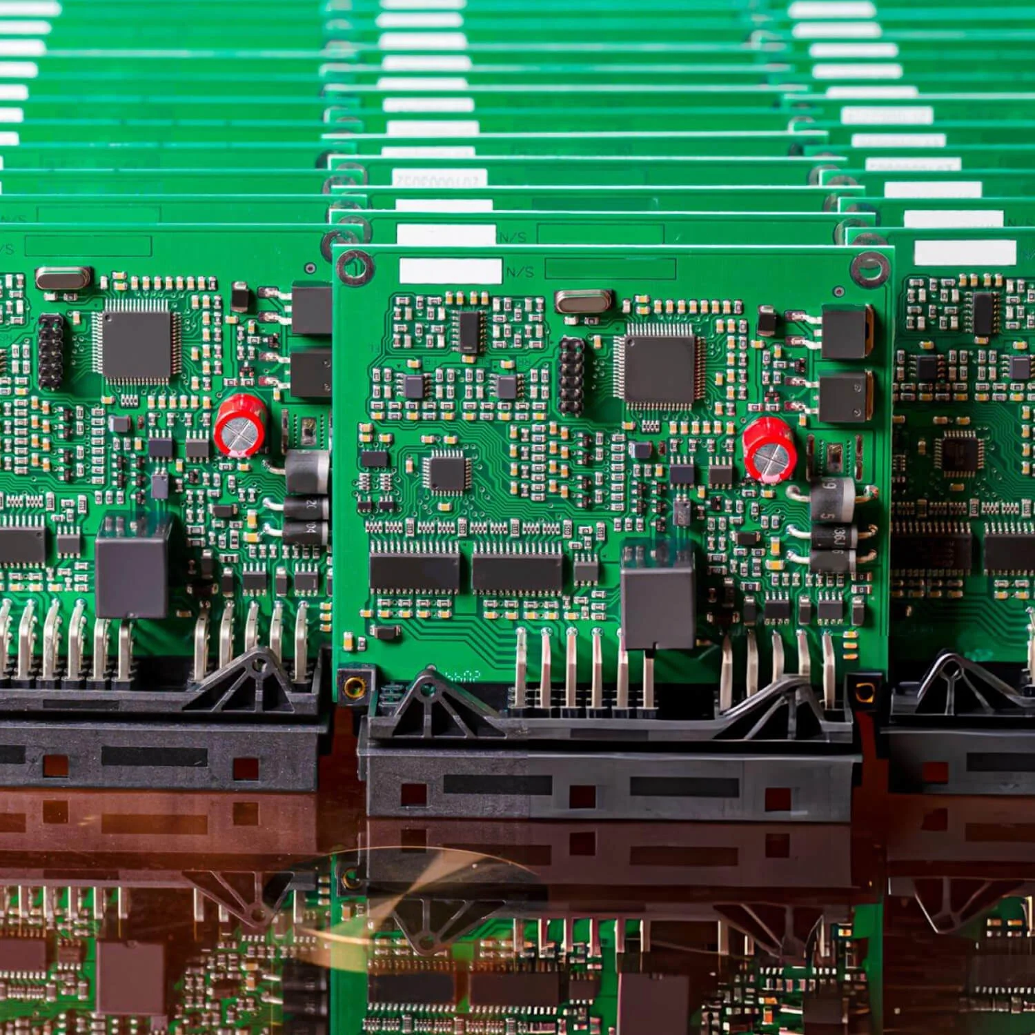
Where a measurement falls outside the expected window, the sample is retained so that the cause can be established before the balance of the batch is released.
FAQ
Can a coverlay be replaced by solder mask on a flex circuit? It can for a static application that is never bent, but solder mask is far less flexible and cracks at a tight radius. Any circuit that will flex should use a coverlay.
What causes adhesive bleed onto pads? Too much adhesive flow during lamination, an opening that is cut too small, or a press cycle that runs too long at temperature. Increasing the opening size slightly and shortening the cycle usually removes it.
How is bond strength verified? By a peel test on a coupon laminated with the same process. The peel force is recorded with the lot, and the value should be compared with the adhesive supplier minimum rather than with a previous batch alone.