In high-speed electronic systems, maintaining predictable signal transmission is essential for reliable performance. As signal frequencies and data rates increase, PCB traces can no longer be treated as simple electrical connections. Their geometry, surrounding dielectric material, reference planes, and transmission distance all influence electrical behavior.
A Controlled Impedance PCB is designed and manufactured so that selected signal traces maintain a specified characteristic impedance. Common target values include 50 Ω for single-ended signals and 90 Ω or 100 Ω for differential interfaces, although the required value depends on the application and interface standard.
Proper PCB Impedance Control helps reduce signal reflections, ringing, crosstalk, and other transmission-line effects. It is therefore widely used in high-speed digital systems, RF circuits, telecommunications equipment, networking hardware, automotive electronics, and other applications where PCB Signal Integrity is critical.
What Is a Controlled Impedance PCB?
A Controlled Impedance PCB is a printed circuit board in which specific traces are designed to achieve a predetermined impedance value. Unlike simple resistance, impedance describes the opposition that a high-frequency signal encounters as it travels along a transmission line.
When a high-speed signal travels through a PCB trace, any sudden change in impedance can cause part of the signal energy to be reflected toward the source. These reflections may lead to waveform distortion, timing errors, data corruption, and electromagnetic interference.
Impedance Control minimizes these discontinuities by controlling the physical and electrical parameters of the transmission line.
The impedance of a PCB trace is primarily determined by:
- Trace width
- Copper thickness
- Distance to the reference plane
- Dielectric constant of the PCB material
- Dielectric thickness
- Trace geometry
- Copper surface characteristics
- Solder mask coverage
- Trace spacing for differential pairs
For example, a designer may specify a 50 Ω single-ended trace or a 100 Ω differential pair. The PCB manufacturer then adjusts the stackup and trace geometry to achieve the required impedance within the specified manufacturing tolerance.
Basic Functions of PCB Impedance Control
PCB Impedance Control plays an important role in high-speed and high-frequency circuit design. Its primary functions include the following.
1. Maintaining Predictable Signal Transmission
Controlled impedance provides a predictable electrical environment for high-speed signals. This allows signals to travel between components with less distortion and fewer reflections.
2. Improving PCB Signal Integrity
Good PCB Signal Integrity is essential for high-speed interfaces. Controlled impedance helps maintain signal quality by reducing impedance discontinuities along critical transmission paths.
3. Reducing Signal Reflections
When the impedance of a transmission line does not match the source, load, or connected components, signal reflections can occur. Properly designed Controlled Impedance traces reduce these reflections and help preserve the intended waveform.
4. Supporting High-Speed Interfaces
Modern interfaces such as Ethernet, USB, PCIe, DDR memory, HDMI, SerDes, and RF communication circuits can require carefully controlled impedance. The exact impedance target depends on the interface and system architecture.
Three Common Types of Controlled Impedance
Controlled impedance structures can generally be divided into single-ended, differential, and coplanar configurations.
1. Single-Ended Controlled Impedance
A single-ended transmission line consists of one signal trace referenced to a nearby ground or power plane.
The impedance is determined by factors such as trace width, copper thickness, dielectric thickness, and dielectric constant.
Single-ended impedance control is commonly used for clock signals, RF signals, and high-speed digital signals.
2. Differential Controlled Impedance
A differential pair consists of two closely spaced traces that carry complementary signals.
In addition to the impedance of each individual trace, the coupling between the two traces affects the overall differential impedance. Therefore, trace width, spacing, distance to the reference plane, and dielectric properties must be controlled carefully.
Common differential impedance targets include 90 Ω and 100 Ω, depending on the interface.
Proper Differential Impedance control is particularly important for high-speed communication interfaces because excessive variation can affect signal quality and timing.
3. Coplanar Controlled Impedance
A coplanar transmission line has a signal trace surrounded by grounded copper on the same PCB layer. It can be implemented as a coplanar waveguide or grounded coplanar waveguide, depending on the presence and arrangement of the reference plane.
This structure is frequently used in RF and microwave designs because it provides additional control over electromagnetic fields and impedance.
Factors That Determine PCB Trace Impedance
The target Controlled Impedance of a PCB trace depends on several physical and material parameters.
1. Trace Width and Copper Thickness
Trace width is one of the most important parameters affecting impedance. In general, increasing trace width changes the characteristic impedance of the transmission line.
Copper thickness also affects the effective geometry of the trace. Therefore, the finished copper thickness should be considered during impedance calculations rather than relying only on the nominal foil thickness.
2. Dielectric Material
The dielectric constant, or Dk, of the PCB material directly influences transmission-line impedance and signal propagation.
Different laminates have different Dk and Df characteristics. For high-speed applications, designers should consider the material’s electrical properties across the relevant frequency range rather than selecting a material based only on its nominal specification.
3. Dielectric Thickness
The distance between the signal trace and its reference plane is another major impedance parameter.
A smaller dielectric spacing generally creates stronger electromagnetic coupling between the trace and reference plane, changing the resulting impedance.
4. Reference Plane
A controlled-impedance trace normally requires a continuous reference plane.
A solid ground plane provides a predictable return-current path and helps maintain consistent impedance. Plane gaps, splits, voids, and other discontinuities can force return current to take a longer path and may degrade signal integrity.
5. Solder Mask
For outer-layer traces, solder mask can affect the effective dielectric environment around the conductor. Depending on the impedance structure and required tolerance, its influence may need to be included in the impedance calculation.
Major Factors Affecting Controlled Impedance
Several factors should be considered when designing and manufacturing a Controlled Impedance PCB.
1. Signal Frequency and Rise Time
Impedance becomes increasingly important as signal frequency and edge rate increase. In fact, a digital signal with a very fast rise or fall time can behave as a high-frequency transmission line even when its clock frequency is relatively low.
Therefore, designers should evaluate signal rise time, trace length, and propagation delay rather than considering frequency alone.
2. Manufacturing Tolerance
Manufacturing variation can affect trace width, copper thickness, dielectric thickness, and material properties.
A common design target may allow approximately ±10% impedance tolerance, while demanding applications may require tighter limits. The appropriate tolerance should be agreed upon between the PCB designer and manufacturer before production.
3. Reference Plane Continuity
The reference plane must remain sufficiently continuous beneath critical high-speed traces.
Routing a high-speed signal across a split plane or large void can interrupt the return-current path and increase electromagnetic radiation and signal distortion.
4. PCB Routing
Trace routing directly influences impedance.
Abrupt changes in trace width, unnecessary neck-down sections, excessive vias, sharp geometry transitions, and poorly designed differential-pair spacing can introduce impedance discontinuities.
Designers should maintain consistent geometry throughout critical transmission paths whenever possible.
5. Material Selection and Stackup
The PCB stackup should be established before final routing.
For a Controlled Impedance PCB, the designer and manufacturer should agree on the dielectric material, copper thickness, dielectric thickness, reference planes, and target impedance before manufacturing data is finalized.
Advantages of Controlled Impedance PCBs
A properly designed Controlled Impedance PCB provides several important advantages for high-speed electronic systems.
1. Improved Signal Integrity
Controlled impedance helps maintain signal quality as signals travel between components, reducing waveform distortion and reflection-related problems.
2. Reduced Signal Reflections
Impedance matching minimizes discontinuities between interconnected transmission lines and components. This is particularly important for high-speed interfaces and long PCB traces.
3. Better High-Speed Performance
With increasing data rates, uncontrolled impedance can become a major limitation. Proper Impedance Control allows high-speed signals to operate more reliably within the electrical design limits of the system.
4. Reduced EMI and Crosstalk Risk
Controlled routing, continuous reference planes, appropriate layer structures, and proper differential-pair design can help reduce unwanted electromagnetic coupling and radiation.
However, impedance control alone does not eliminate EMI. It should be combined with good grounding, return-path design, layer stackup, filtering, shielding, and overall EMC design practices.
5. Improved System Reliability
Maintaining consistent transmission-line characteristics can reduce signal-integrity failures during development and production, helping improve the reliability of communication and high-speed electronic systems.
How Is Controlled Impedance Calculated?
Impedance calculations are normally performed using PCB field-solver software or specialized impedance calculators.
The calculation typically considers:
- Trace width
- Trace thickness
- Dielectric thickness
- Dielectric constant
- Trace-to-plane distance
- Differential-pair spacing
- Copper geometry
- Solder mask
- PCB stackup
For differential structures, the software also calculates the electromagnetic coupling between the two traces.
A Smith chart can be useful for RF and microwave circuit analysis, but it is not itself the primary method for calculating the physical trace impedance of a typical PCB transmission line. Modern PCB impedance design generally relies on transmission-line equations and electromagnetic field-solver tools.
Common Mistakes in Controlled Impedance PCB Design
1. Incorrect Stackup Information
One of the most common mistakes is designing impedance traces without confirming the actual PCB stackup.
The designer should define the signal layer, reference plane, dielectric thickness, copper thickness, and material properties before routing critical traces.
2. Incorrect Trace Width
If the calculated trace width does not match the manufacturer’s actual process capability, the finished PCB may not achieve the required impedance.
The target should therefore be designed around the manufacturer’s realistic fabrication tolerances.
3. Poor Differential-Pair Spacing
For differential signals, the spacing between the two traces affects coupling and therefore the resulting differential impedance.
The width and spacing of the pair should be controlled consistently along the entire critical routing path.
4. Interrupted Reference Planes
Routing a controlled-impedance signal across a split or discontinuous reference plane can create an unfavorable return-current path.
This can cause impedance discontinuities, increased crosstalk, and greater EMI risk.
5. Excessive Routing Changes
Frequent changes in trace width, unnecessary vias, sharp transitions, and inconsistent geometry can introduce discontinuities.
Critical high-speed routes should be kept as uniform as practical.
6. Unrealistic Impedance Tolerances
Specifying an unnecessarily tight impedance tolerance can increase manufacturing difficulty and cost without providing meaningful system-level benefits.
The impedance tolerance should be based on the electrical requirements of the application and the actual capabilities of the PCB manufacturer.
Applications of Controlled Impedance PCBs
Controlled Impedance PCB technology is widely used in applications where signal quality and transmission performance are critical.
Common applications include:
- Telecommunications equipment
- Networking and data communication systems
- High-speed digital electronics
- RF and microwave equipment
- Automotive electronics
- Industrial control systems
- Medical electronics
- Computer and server hardware
- Video and imaging systems
- High-speed computing platforms
- Wireless communication equipment
- Test and measurement equipment
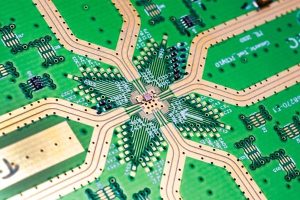
Kingda: Controlled Impedance PCB Manufacturing
For a Controlled Impedance PCB, successful manufacturing requires close coordination between PCB design and production engineering.
Kingda can support impedance-controlled PCB projects by working with customers on critical design and manufacturing parameters, including PCB stackup, material selection, trace geometry, copper thickness, dielectric construction, and impedance requirements.
A professional manufacturing process should verify the design data before production and ensure that the selected stackup and fabrication parameters are consistent with the required impedance targets.
For demanding high-speed and RF applications, impedance control should be considered from the beginning of the PCB design process rather than added after routing is completed.
By combining appropriate material selection, controlled stackup design, manufacturable trace geometry, process control, and electrical testing, manufacturers can help customers achieve reliable PCB Signal Integrity and consistent Controlled Impedance performance.
Conclusion
As electronic systems continue to operate at higher speeds and data rates, PCB Impedance Control has become an important part of modern PCB design and manufacturing.
A Controlled Impedance PCB is not simply a circuit board with a specified resistance value. Its impedance is determined by the interaction between trace geometry, dielectric materials, reference planes, copper thickness, routing structure, and manufacturing tolerances.
For high-speed digital, RF, telecommunications, networking, and other signal-sensitive applications, controlling these parameters can reduce reflections, improve signal integrity, and increase system reliability.
Working closely with an experienced PCB manufacturer such as Kingda during the stackup, routing, and manufacturing stages can help ensure that impedance requirements are practical, measurable, and consistently achieved.