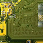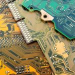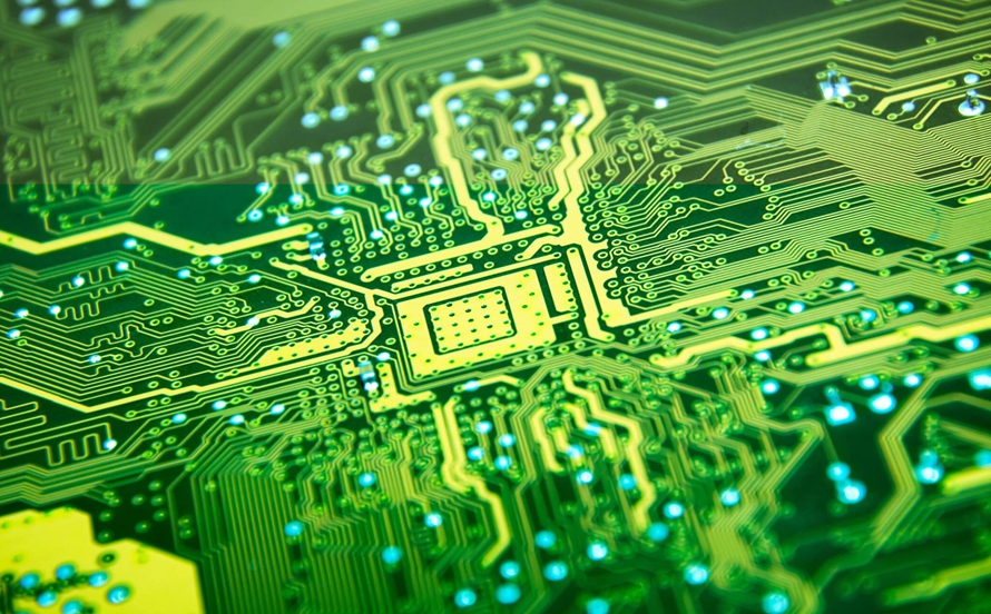
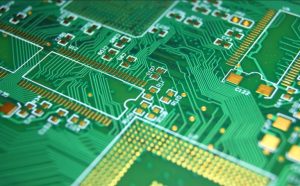
A Bare PCB, also called a bare circuit board or unassembled PCB, is a fully fabricated printed circuit board without electronic components mounted on it. It contains the conductive copper patterns, dielectric materials, vias, pads, solder mask, surface finish, and other structures required to form the electrical connections defined by the PCB design.
Although a Bare Circuit Board cannot perform its intended electronic function until components are assembled, it is a critical stage in the electronics manufacturing process. Many manufacturing inspections and electrical tests are performed before component assembly. Verifying the bare board at this stage helps identify manufacturing defects before additional assembly costs are introduced.
A bare PCB is therefore the foundation of the finished PCBA and plays an important role in product reliability, manufacturability, and signal integrity.
What Is a Bare PCB?
A Bare PCB is a manufactured PCB that contains no electronic components such as integrated circuits, resistors, capacitors, connectors, or switches.
Depending on the design, a bare board may include:
- Copper signal traces
- Power and ground planes
- Through-hole vias
- Blind and buried vias
- Component pads
- Solder mask
- Silkscreen or legend
- Surface finish
- Edge connectors or gold fingers
- Mounting holes
- Test points
The board itself does not execute the circuit’s intended function until components are installed. However, it can undergo dimensional inspection, visual inspection, electrical testing, impedance verification, and other manufacturing checks before assembly.
Main Components of a Bare PCB
A typical Bare Circuit Board consists of several structural and functional elements.
1. Substrate or Base Material
The substrate provides mechanical support and electrical insulation between conductive layers.
Common PCB materials include FR-4, high-Tg laminates, flexible polyimide, high-frequency laminates, metal-core materials, and other specialized dielectric systems.
The material is selected according to electrical performance, thermal requirements, mechanical conditions, operating temperature, and application requirements.
2. Copper Layers
Copper forms the conductive structure of the PCB.
Depending on the design, copper layers may function as:
- Signal layers
- Power planes
- Ground planes
- Internal routing layers
- Component connection areas
The required copper thickness depends on current capacity, thermal requirements, mechanical considerations, and manufacturing capability.
3. Solder Mask
Solder mask is a protective insulating coating applied over selected areas of the copper surface.
It helps protect copper from oxidation, reduces the risk of solder bridging during assembly, and provides electrical insulation between exposed conductive areas.
4. Silkscreen
The silkscreen, also called the legend, contains reference designators, polarity marks, component identifiers, logos, warning symbols, and other manufacturing information.
White is commonly used, although other colors can be specified depending on the manufacturing process and design requirements.
5. Surface Finish
The surface finish is applied to exposed copper areas such as component pads, contacts, and other solderable surfaces.
Common finishes include:
- HASL
- Lead-free HASL
- ENIG
- ENEPIG
- Immersion tin
- Immersion silver
- OSP
- Hard gold for contact areas
The appropriate finish depends on solderability, storage requirements, contact durability, environmental conditions, cost, and assembly requirements.
Bare PCB vs. Zero PCB
A Bare PCB should not be confused with a zero PCB, also commonly referred to as a prototyping board or universal PCB.
A bare PCB is a custom-manufactured circuit board produced according to a specific electronic design. Its copper traces, pads, vias, layer structure, and other features are defined by the circuit design.
A zero PCB, by comparison, is a general-purpose prototyping board. It normally contains a regular grid of holes and is designed for manually connecting components using wires, solder bridges, or other methods.
The main differences are:
| Feature | Bare PCB | Zero PCB |
|---|---|---|
| Design | Custom circuit design | General-purpose grid |
| Copper routing | Designed according to the circuit | Usually no predefined circuit routing |
| Solder mask | Normally available | Usually not present |
| Silkscreen | Normally available | Usually limited or absent |
| Main purpose | Final electronic product | Prototyping and experimentation |
| Manufacturing | Professional PCB fabrication | Standard off-the-shelf board |
A zero PCB is useful for testing simple circuits, while a Bare Circuit Board is the foundation for a specific electronic product.
Bare PCB Manufacturing Process
The Bare PCB Manufacturing process involves multiple controlled steps. The exact sequence varies depending on the PCB structure, layer count, materials, surface finish, HDI technology, and production requirements.
1. PCB Design and Manufacturing Data Preparation
The process begins with the circuit schematic and PCB layout.
Engineers use EDA software to create the PCB design and perform design rule checks (DRC). Depending on the application, signal integrity, power integrity, thermal, and other simulations may also be performed.
Manufacturing data may include:
- Gerber files
- Drill files
- NC drill data
- Stackup information
- Fabrication drawings
- Impedance requirements
- Surface finish requirements
- Special manufacturing instructions
The manufacturer reviews the files through DFM analysis before production begins.
2. Artwork and Film Preparation
For traditional PCB manufacturing processes, the production data is converted into artwork used to transfer circuit patterns onto the copper-clad material.
Each relevant PCB layer requires its corresponding imaging data. Depending on the manufacturing technology, modern PCB factories may use direct imaging rather than conventional film-based imaging.
The purpose is the same: accurately transfer the designed circuit pattern to the PCB material.
3. Inner-Layer Imaging
For a multilayer PCB, the inner copper layers are prepared first.
A photosensitive material is applied to the copper surface. The circuit image is then transferred using the appropriate imaging process.
After development, the unwanted areas of copper can be removed through controlled chemical etching, leaving the required circuit pattern.
4. Inner-Layer Inspection
Each inner layer is inspected before lamination.
Automated optical inspection (AOI) can compare the manufactured copper pattern with the original design data and identify potential defects such as:
- Missing traces
- Excess copper
- Open circuits
- Shorts
- Pattern deformation
- Incorrect features
Detecting defects before lamination is important because repairing a defect after multilayer assembly can be significantly more difficult.
5. Layer Stacking and Lamination
The prepared inner layers are stacked together with dielectric materials such as prepreg and copper foil according to the specified PCB stackup.
The stack is then subjected to controlled temperature and pressure in a lamination press.
During lamination, the resin in the prepreg flows and cures, bonding the layers into a single multilayer structure.
Precise control of temperature, pressure, heating rate, resin flow, and cooling is important for dimensional stability and reliable interlayer connections.
6. Drilling
After lamination, holes are drilled according to the manufacturing data.
Depending on the design, drilling may create:
- Through holes
- Via holes
- Component holes
- Mechanical holes
- Back-drilled structures
High-density PCBs may additionally use laser drilling to create microvias.
Drilling accuracy is particularly important for multilayer and HDI PCBs because each hole must connect to the intended copper layers.
7. Copper Plating
After drilling, the exposed hole walls must be made electrically conductive.
The PCB undergoes cleaning and chemical preparation, followed by electroless copper deposition. This creates an initial conductive layer on the hole walls.
Additional electrolytic copper plating then increases the copper thickness on the board surface and inside the holes.
Reliable copper plating is essential for maintaining electrical continuity and mechanical reliability of plated-through holes and vias.
8. Outer-Layer Circuit Formation
The outer-layer circuit pattern is transferred onto the PCB.
Depending on the manufacturing process, imaging, plating, etching, and tin-resist processes are used to form the final copper pattern.
The unwanted copper is removed while the required circuit features are protected.
9. Final Etching
The PCB undergoes controlled etching to remove unwanted exposed copper.
The remaining copper forms the final signal traces, pads, planes, and other conductive features.
The boards are then cleaned to remove chemical residues before continuing to the next process.
10. Solder Mask Application
A solder mask coating is applied to the PCB surface.
After exposure and development, the required pad and contact areas remain exposed while most other copper is protected.
The solder mask helps prevent accidental solder bridging, protects the copper surface, and improves the long-term durability of the board.
11. Surface Finish
An appropriate surface finish is applied to exposed copper areas.
The selection depends on the intended assembly process and product requirements.
For example, ENIG is commonly used for fine-pitch SMT applications, while hard gold may be selected for PCB edge contacts that experience repeated mechanical insertion.
12. Silkscreen Printing
The PCB legend is printed on the board surface.
Reference designators, polarity indicators, logos, and other required markings are added according to the manufacturing data.
13. Electrical Testing
Electrical testing is performed to verify that the manufactured board corresponds to the intended electrical design.
Depending on the PCB type and customer requirements, testing may include continuity, isolation, shorts, opens, and impedance verification.
14. PCB Profiling and Depanelization
PCBs are often manufactured in panels containing multiple individual boards.
After the required inspections and tests are completed, the individual boards are separated from the manufacturing panel using methods such as:
- CNC routing
- V-scoring
- Punching
- Laser cutting for specialized applications
The final Bare PCB is then ready for shipment to the assembly stage.
Electrical Testing of Bare PCBs
Electrical testing is an important part of PCB Testing because manufacturing defects may not always be visible during visual inspection.
Testing requirements depend on PCB complexity, application, customer specifications, and applicable industry standards.
Common electrical tests include the following.
1. Resistance Testing
Resistance measurements can help verify the electrical characteristics of conductive paths and detect abnormal resistance caused by manufacturing problems.
For specialized applications, resistance measurements may be used to evaluate specific low-resistance paths.
2. Isolation Testing
Isolation testing checks whether separate electrical networks are adequately insulated from each other.
This helps identify unintended conductive paths and potential short circuits between isolated nets.
3. Capacitance Testing
Capacitance measurements may be used for specialized PCB verification and can help evaluate electrical characteristics between selected conductors.
This type of testing is more application-dependent than basic continuity and isolation testing.
4. Continuity Testing
Continuity testing verifies that intended electrical connections are complete.
It checks whether nodes belonging to the same electrical net have the expected conductive path and helps identify open circuits.
5. Short-Circuit Testing
Short testing verifies that electrically separate nets are not unintentionally connected.
This is particularly important for dense multilayer and fine-line PCBs, where small manufacturing defects can create unwanted connections.
6. Impedance Testing
For high-speed PCBs, impedance verification may be required to confirm that designated transmission lines meet the specified impedance target.
This is particularly important for applications involving high-speed digital signals, RF circuits, and differential interfaces.
7. Flying Probe Testing
Flying probe testing uses movable probes to contact specific test points on the PCB.
It can verify continuity and isolation without requiring a dedicated fixture, making it especially useful for prototypes, small batches, and products that undergo frequent design changes.
8. Four-Wire Kelvin Testing
A four-wire Kelvin measurement is used when highly accurate low-resistance measurements are required.
Because the method minimizes the influence of test-lead resistance, it can be useful for specialized high-current or low-resistance applications. It is not normally required for every standard PCB.
Why Is Bare PCB Testing Important?
Testing the board before component assembly provides several benefits.
First, it prevents defective boards from entering the SMT or through-hole assembly process. This avoids spending additional assembly costs on a PCB that already contains a manufacturing defect.
Second, electrical testing can detect problems that may not be visible through visual inspection alone.
Third, early verification helps manufacturers identify process problems and improve production consistency.
For high-reliability applications, combining visual inspection, AOI, dimensional inspection, electrical testing, and other appropriate verification methods provides a more comprehensive quality-control process.
Common Bare PCB Manufacturing Defects
During Bare PCB Manufacturing, several types of defects can affect board performance.
Common problems include:
- Open circuits
- Short circuits
- Insufficient copper plating
- Excessive copper
- Plating voids
- Poor solder mask registration
- Incorrect hole size
- Drill misalignment
- Layer-to-layer registration errors
- Surface-finish defects
- Board warpage
- Delamination
- Trace width variation
Effective process control, DFM review, automated inspection, and electrical testing help reduce these risks.
Kingda: Your Bare PCB Manufacturing Partner
Kingda provides PCB manufacturing solutions for customers requiring reliable Bare PCB Manufacturing.
From engineering review and manufacturing data verification to PCB fabrication, inspection, electrical testing, and final processing, each stage should be coordinated with the customer’s design requirements.
For complex PCB projects, key manufacturing factors may include:
- Multilayer PCB fabrication
- High-density interconnect structures
- Controlled impedance
- Fine-line routing
- Different copper thicknesses
- Advanced surface finishes
- Blind and buried vias
- High-Tg materials
- High-frequency materials
- Specialized PCB structures
Kingda focuses on engineering communication and manufacturing process control to help customers convert PCB designs into manufacturable, reliable circuit boards.
A well-controlled manufacturing process can also reduce the risk of defects reaching the assembly stage and help improve overall product development efficiency.
Conclusion
A Bare PCB is much more than an unfinished circuit board. It is the fully fabricated foundation on which electronic components are subsequently assembled to create a functional PCBA.
From material selection and circuit imaging to lamination, drilling, copper plating, solder mask, surface finishing, and PCB Testing, every stage of the PCB Manufacturing Process affects the final electrical and mechanical performance of the board.
Proper inspection and electrical verification are especially important before assembly. By identifying manufacturing defects at the bare-board stage, manufacturers can reduce assembly risks, improve production efficiency, and support more reliable electronic products.
For demanding applications, choosing an experienced manufacturing partner and involving the manufacturer early in the design and DFM process can help ensure that the finished Bare Circuit Board meets the required electrical, mechanical, and manufacturing specifications.