What Is a Microvia PCB?
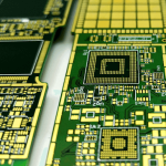
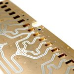
A Microvia PCB is a printed circuit board that uses extremely small vias to create high-density interconnections between PCB layers. Microvias are particularly important in high-density electronic products where conventional through-holes would consume too much routing space.
In PCB manufacturing, a microvia is generally understood as a very small via, commonly with a finished diameter of approximately 150 μm (6 mil) or less. The exact definition may vary according to the applicable industry standard and manufacturing process.
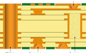
Unlike conventional plated through-holes (PTHs), which normally extend through the entire PCB, microvias are typically formed as blind structures connecting an outer layer to an adjacent or nearby inner layer. They are commonly manufactured using laser drilling and are a fundamental technology in HDI PCB manufacturing.
As electronic products become smaller, thinner, lighter, and more powerful, microvia technology has become increasingly important. Smartphones, wearable devices, IoT equipment, portable cameras, automotive electronics, medical devices, and other compact products can all benefit from microvia-based interconnection structures.
Why Are Microvias Important in PCB Design?
Traditional through-holes extend through multiple PCB layers. Even when a connection only requires two specific layers, the through-hole occupies space on every layer it passes through.
This can create routing restrictions in high-density PCB designs.
Microvias solve this problem by creating shorter and more localized interconnections. Designers can connect specific layers without sacrificing as much routing space on other layers.
The major benefits include:
- Higher interconnection density
- More efficient use of PCB space
- Smaller PCB dimensions
- Better component escape routing
- Improved flexibility in multilayer stack-up design
- Support for fine-pitch BGA and CSP packages
- Reduced dependence on large mechanical through-holes
- Greater design freedom for compact electronic products
For these reasons, microvias are especially valuable in HDI PCB structures.
Main Types of Microvias in PCB Manufacturing
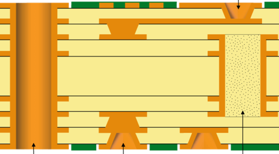
Microvia technology can be implemented in several different structures. The most common structures include blind microvias, buried vias, stacked vias, staggered vias, and any-layer via structures.
Blind Microvias
A Blind Via connects an outer copper layer to one or more inner layers without passing completely through the PCB.
For example, in a multilayer board, an L1–L2 microvia connects the first layer to the second layer, while an L1–L3 structure can connect the first layer to the third layer when the manufacturing process supports the required depth.
Blind microvias are widely used for component escape routing, particularly beneath or around fine-pitch BGA packages.
Laser drilling is commonly used because it can create very small holes with controlled depth and high positional accuracy.
Buried Vias
A Buried Via is located entirely within the internal layers of a multilayer PCB. It does not connect to either the top or bottom external surface.
For example, in an eight-layer PCB, a via connecting L3 and L4 can be completely buried inside the board.
Buried vias provide additional routing resources because they do not occupy external-layer space. However, they normally require more complicated fabrication processes, such as sequential lamination, which can increase manufacturing cost and process complexity.
Stacked Microvias
Stacked microvias are microvias positioned vertically on top of one another.
For example, a microvia connecting L1–L2 can be stacked with another microvia connecting L2–L3. After appropriate copper filling and plating, the structures form a vertical interconnection through multiple layers.
Stacked microvias are useful when designers need to connect several HDI layers while maintaining a compact footprint.
Because the reliability of stacked structures depends heavily on copper filling, plating quality, layer registration, and thermal-mechanical stresses, they require carefully controlled manufacturing processes.
Staggered Microvias
Staggered microvias also connect multiple layers, but the individual microvias are offset rather than placed directly on top of one another.
For example, an L1–L2 microvia and an L2–L3 microvia may be positioned with a horizontal offset.
Compared with stacked structures, staggered microvias can provide different manufacturing and reliability advantages depending on the stack-up and design requirements.
The appropriate structure should be selected based on PCB density, component pitch, electrical requirements, manufacturing capability, and reliability targets.
Any-Layer Microvias
Any-layer technology represents an advanced form of HDI interconnection in which microvias can be formed between successive layers throughout the PCB stack-up.
Instead of restricting blind vias to a specific outer-layer structure, any-layer HDI technology allows designers to establish highly flexible layer-to-layer connections.
For example, an eight-layer any-layer HDI PCB may use sequential lamination and laser drilling to progressively build interconnections between adjacent layers.
This approach can significantly increase routing flexibility and is especially useful for extremely compact and high-density products.
However, any-layer PCB manufacturing requires highly accurate equipment, advanced process control, precise registration, and experienced engineering teams.
Microvia vs. Conventional PTH
It is important to distinguish microvias from conventional plated through-holes.
| Feature | Microvia | Conventional PTH |
|---|---|---|
| Typical Diameter | Very small, often ≤150 μm | Generally larger |
| Structure | Usually blind | Usually through-hole |
| Drilling Method | Commonly laser | Commonly mechanical drilling |
| Layer Connection | Specific layers | Can connect multiple layers |
| Space Usage | Low | Higher |
| Typical Application | HDI, BGA, compact electronics | Standard multilayer PCBs |
| Manufacturing Complexity | Higher | Relatively lower |
A small mechanically drilled hole is not automatically considered a microvia. Microvia classification depends on factors such as structure, diameter, depth, and manufacturing technology.
This distinction is important when establishing PCB design rules and manufacturing specifications.
VIPPO: Via-in-Pad Plated Over
VIPPO stands for Via-In-Pad Plated Over. It is an advanced PCB structure in which a via is placed directly inside a component pad and then filled and covered with copper.
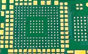
VIPPO is particularly useful for fine-pitch BGA packages because it allows the via to occupy the pad area instead of consuming additional routing space around the component.
A typical VIPPO process includes:
- Drilling the via inside the pad.
- Filling the via with a suitable material.
- Planarizing the surface.
- Plating over the filled via.
- Finishing the surface to create a suitable soldering pad.
The resulting surface is substantially flatter than an open via.
Properly manufactured VIPPO structures can help prevent solder from flowing into the via during PCB assembly and can improve BGA soldering reliability.
Via filling and planarization quality are therefore critical. Poorly filled or improperly plated vias can create soldering defects, voids, surface irregularities, or reliability problems.
Microvia PCB Applications
Microvia technology is widely used in electronic products where high circuit density and compact dimensions are important.
Typical applications include:
- Smartphones
- Smartwatches and wearable devices
- Wireless communication equipment
- IoT devices
- Portable cameras
- Virtual reality equipment
- Automotive electronics
- Medical electronics
- Industrial control systems
- High-performance computing equipment
- Networking equipment
- Aerospace electronics
- Compact consumer electronics
In particular, microvias provide significant advantages when routing signals from fine-pitch BGA, CSP, and other miniature packages.
Microvia PCB Manufacturing Methods
Several technologies can be used to create small holes and microvia structures during PCB production.
The most important methods include mechanical drilling, laser drilling, plasma processing, and chemical processes.
Mechanical Drilling
Mechanical drilling uses high-speed drilling equipment equipped with precision tools, commonly carbide drill bits.
Carbide tools provide high hardness and wear resistance and are widely used for conventional PCB hole drilling.
Mechanical drilling remains an important PCB manufacturing process, but it becomes increasingly difficult as hole diameter decreases. Very small drill bits are more susceptible to breakage and deflection, while high aspect ratios can make reliable copper plating more challenging.
Therefore, mechanical drilling is generally more suitable for conventional through-holes and larger vias than extremely small microvias.
Laser Drilling
Laser Drilling is one of the most important technologies for modern microvia production.
Laser systems can create very small holes by selectively removing dielectric material and, depending on the process, interacting with the underlying copper structure.
Common laser technologies include:
- CO₂ lasers
- UV lasers
- UV/YAG laser systems
- Excimer laser systems
The optimal laser wavelength and processing parameters depend on the dielectric material, copper thickness, via diameter, required depth, and PCB stack-up.
Laser drilling offers several important advantages:
- Extremely small hole diameters
- High positional accuracy
- Controlled drilling depth
- High processing density
- Excellent suitability for HDI structures
- Compatibility with fine-pitch component routing
For this reason, laser drilling has become a core process in advanced HDI PCB manufacturing.
Plasma Etching
Plasma processing can be used for specialized PCB applications where conventional drilling methods are difficult to apply.
A controlled plasma environment can remove selected dielectric materials through physical and chemical interactions. Plasma processing may be useful for certain high-density interconnection structures and specialized materials.
However, plasma etching is a specialized process and is not a direct replacement for laser drilling in every microvia application.
Chemical Processing
Chemical processes can be used in specialized PCB fabrication processes to selectively remove or modify materials.
The process involves controlled chemical reactions with specific layers or materials. Because chemical processing requires precise control of chemistry, temperature, exposure time, and material compatibility, it is generally applied only where the process is technically appropriate.
For mainstream microvia production, laser drilling is generally the more important technology.
Key Microvia PCB Manufacturing Challenges
Producing reliable microvias requires much tighter process control than conventional PCB fabrication.
Via Diameter and Depth Control
Small deviations in via diameter or depth can affect electrical connectivity and plating reliability.
The drilling process must therefore be accurately matched to the dielectric thickness and intended interconnection structure.
Copper Plating
Copper plating is critical for microvia reliability.
The copper layer must provide a continuous electrical connection while maintaining adequate mechanical strength. For stacked microvias, copper filling and plating quality become even more important because multiple microvia structures may experience thermal and mechanical stress during PCB assembly and operation.
Layer Registration
As the number of sequential lamination and drilling operations increases, registration accuracy becomes increasingly important.
Even a small alignment error can reduce the available capture pad area or cause an electrical connection failure.
Lamination
Advanced HDI structures often require sequential lamination.
The manufacturer must carefully control:
- Resin flow
- Lamination temperature
- Lamination pressure
- Material thickness
- Layer alignment
- Dimensional stability
- Copper distribution
Poor lamination control can result in voids, delamination, warpage, or registration problems.
Reliability Testing
Microvia structures should be evaluated according to the expected application requirements.
Depending on the product, testing may include:
- Electrical continuity testing
- Insulation resistance testing
- Thermal cycling
- Microsection analysis
- Solderability testing
- Thermal stress testing
- Plating inspection
- Dimensional inspection
For automotive, medical, aerospace, and other high-reliability applications, additional qualification requirements may apply.
Microvia PCB Design Considerations
A successful Microvia PCB design requires close coordination between the PCB designer and manufacturer.
Before finalizing the layout, engineers should confirm:
- Minimum microvia diameter
- Microvia depth
- Aspect ratio
- Capture pad diameter
- Pad-to-via spacing
- Via-to-trace clearance
- Copper thickness
- Dielectric thickness
- Laser drilling capability
- Stacked or staggered microvia capability
- Sequential lamination requirements
- Via filling requirements
- Surface finish
- Required reliability level
Designers should avoid using unnecessarily small microvias when larger structures can meet the electrical and mechanical requirements. A practical design that matches the manufacturer’s process capability can improve yield, reliability, and overall cost efficiency.
Kingda Microvia PCB Manufacturing Capabilities
Kingda provides advanced PCB manufacturing solutions for high-density and complex electronic applications.
Our microvia-related capabilities include:
| Capability | Specification |
|---|---|
| Materials | Rigid, Flexible, Rigid-Flex, High-Frequency, High-Speed, High-Tg, Ceramic |
| Via Types | Blind Vias, Buried Vias, Microvias, Stacked Vias, Staggered Vias, Any-Layer Vias, VIPPO, Backdrilling |
| Via Filling | Epoxy Resin, Copper, Silver, Solder Mask Ink |
| Surface Finishes | ENIG, Immersion Silver, Immersion Tin, OSP, ENEPIG, Gold Plating |
| Layer Count | 1–40 layers, with special constructions available |
| Board Thickness | 0.13–7.0 mm |
| Maximum Board Size | Up to 21 × 59 in |
| Maximum Aspect Ratio | Up to 16:1 for drilled holes ≥0.2 mm |
| Typical Lead Time | 2–4 weeks |
Actual capabilities may vary depending on material selection, layer count, board thickness, via structure, aspect ratio, and overall stack-up.
Why Choose Kingda for Microvia PCB Manufacturing?
As electronic products continue to become smaller and more functionally integrated, high-density interconnection technology is becoming increasingly important.
Kingda supports customers with advanced multilayer and HDI PCB requirements, including Microvia PCB structures, blind vias, buried vias, stacked microvias, staggered microvias, any-layer interconnections, and VIPPO solutions.
Our engineering and manufacturing processes focus on critical factors such as:
- Stack-up optimization
- Material selection
- Laser drilling
- Mechanical drilling
- Copper plating
- Via filling
- Sequential lamination
- Layer registration
- Surface finishing
- Electrical testing
- Reliability verification
By considering manufacturing capability during the PCB design stage, customers can achieve higher routing density while maintaining electrical performance, mechanical reliability, production yield, and cost control.
Conclusion
A Microvia PCB is an important solution for high-density and miniaturized electronic products. By using extremely small interconnection structures, microvias allow designers to make more efficient use of limited PCB space and support increasingly fine-pitch components.
HDI PCB technology commonly combines Microvia, Blind Via, and Buried Via structures with sequential lamination and Laser Drilling to achieve high interconnection density.
Advanced structures such as stacked microvias, staggered microvias, any-layer vias, and VIPPO further expand the design possibilities for compact and high-performance electronics.
Although microvia manufacturing is more complex than conventional through-hole PCB fabrication, careful stack-up design, accurate drilling, reliable copper plating, precise registration, and strict process control can produce highly reliable interconnections.
For applications requiring smaller dimensions, higher circuit density, and advanced component packaging, microvia technology provides an effective foundation for next-generation PCB design and manufacturing.