What Is a High-Frequency PCB?
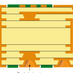
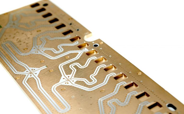
A High-Frequency PCB is a printed circuit board designed to transmit and process high-frequency electrical signals while maintaining stable electrical performance, controlled impedance, and low signal loss.
High-frequency PCBs are commonly used in applications involving RF, microwave, wireless communication, radar, satellite communication, automotive sensing, medical equipment, and other advanced electronic systems.
Unlike conventional PCBs, high-frequency designs are more sensitive to material properties, transmission-line geometry, dielectric thickness, copper surface roughness, impedance control, and electromagnetic coupling. As operating frequencies increase, even small variations in PCB construction can affect signal attenuation, phase characteristics, reflections, and overall system performance.
High-frequency PCB technology has therefore become increasingly important for modern communication and electronic systems, particularly as wireless networks, radar, satellite communications, and high-speed data transmission continue to evolve.
Main Characteristics of High-Frequency PCBs
The electrical and mechanical performance of a high-frequency PCB depends heavily on material selection and controlled manufacturing processes.
Several key factors should be considered.
Low Dielectric Constant (Dk)
The dielectric constant, or Dk, affects the propagation velocity and electrical behavior of signals traveling through the PCB dielectric.
A lower and more stable Dk can be advantageous for certain high-frequency applications because it can support faster signal propagation and help reduce electrical length. However, higher is not necessarily better or worse. The appropriate Dk depends on the required impedance, stack-up, signal wavelength, circuit geometry, and application.
Dk stability across frequency, temperature, and material lot is also important for consistent RF performance.
Low Dissipation Factor (Df)
Df, also called the dissipation factor or loss tangent, indicates how much energy is lost within the dielectric material.
For demanding RF and microwave applications, a low Df is generally preferred because it helps reduce dielectric loss and signal attenuation.
As operating frequency increases, material loss becomes increasingly important. Therefore, selecting appropriate High-Frequency PCB Materials is essential for maintaining signal quality.
Controlled Dielectric Thickness
Dielectric thickness directly affects transmission-line impedance.
Small variations in dielectric thickness can change the impedance of microstrip and stripline structures. Therefore, consistent dielectric thickness and accurate lamination control are important for high-frequency PCB manufacturing.
Thermal Stability
High-frequency materials must maintain stable electrical characteristics over the expected operating temperature range.
Temperature changes can affect Dk, Df, physical dimensions, and impedance. A material with good thermal stability can help maintain predictable circuit performance.
Low Moisture Absorption
Moisture can affect dielectric properties and dimensional stability.
Materials with low moisture absorption are often preferred for demanding RF and microwave applications because they help maintain more consistent electrical performance under changing environmental conditions.
Copper Surface Roughness
Copper roughness can become an important factor at high frequencies because current tends to concentrate near the conductor surface due to the skin effect.
Excessive copper roughness can increase conductor loss. Therefore, copper foil selection and surface treatment should be considered together with the target frequency and transmission-line design.
Benefits of High-Frequency PCBs
A properly designed high-frequency PCB can provide several advantages for advanced electronic systems.
High-Speed Signal Transmission
High-frequency PCBs are designed to maintain controlled electrical characteristics at elevated operating frequencies.
With appropriate materials, stack-up design, impedance control, and routing techniques, they can support fast and stable signal transmission.
Excellent Signal Integrity
Signal Integrity is one of the most important considerations in high-frequency PCB design.
Proper material selection and transmission-line design can help control:
- Signal attenuation
- Reflection
- Crosstalk
- Insertion loss
- Return loss
- Phase variation
- Electromagnetic coupling
Maintaining signal integrity becomes increasingly difficult as frequency and data rates increase, making controlled PCB construction essential.
Stable Impedance
High-frequency circuits often use controlled-impedance transmission lines.
Common configurations include microstrip, stripline, coplanar waveguide, and other RF transmission structures. Their impedance depends on conductor width, copper thickness, dielectric thickness, Dk, and surrounding geometry.
Compact Circuit Integration
High-frequency circuits can support compact RF and communication modules when the PCB stack-up and routing are optimized appropriately.
However, smaller dimensions should not be treated as an automatic consequence of using high-frequency materials. Overall product size depends on the complete circuit, component selection, thermal requirements, mechanical design, and packaging strategy.
Reliable RF Performance
When materials and manufacturing tolerances are properly controlled, high-frequency PCBs can provide stable RF performance for demanding communication, radar, sensing, and microwave applications.
High-Frequency PCB Materials
Material selection is one of the most important aspects of High-Frequency PCB Design.
Traditional FR-4 can be used for certain relatively low-frequency or mixed-signal applications, but specialized high-frequency laminates may be required as frequency increases or when low loss and stable dielectric properties become critical.
Common material categories include:
PTFE-Based Materials
PTFE-based laminates offer low dielectric loss and are widely used in RF and microwave applications.
They can provide excellent high-frequency electrical performance but may require specialized processing because of their mechanical and thermal characteristics.
High-Frequency Hydrocarbon/Ceramic Materials
These materials can provide a balance between RF performance, mechanical stability, manufacturability, and cost.
They are commonly considered for communication, RF, antenna, and microwave applications.
High-Tg FR-4 and Advanced FR-4
For mixed-frequency designs, advanced FR-4 or high-Tg FR-4 may be combined with specialized high-frequency materials.
This type of hybrid construction can be useful when one PCB contains both conventional digital circuitry and high-frequency RF sections.
Material selection should always be based on the actual operating frequency, Dk/Df requirements, thermal conditions, fabrication process, and reliability requirements.
High-Frequency PCB Design Considerations
Designing a high-frequency circuit requires more than simply selecting a high-frequency laminate.
1. Material Selection
Select materials according to:
- Operating frequency
- Dk
- Df
- Thermal stability
- Moisture absorption
- CTE
- Copper compatibility
- Mechanical requirements
- Manufacturing capability
The selected material should provide predictable electrical characteristics across the expected frequency and temperature range.
2. Impedance Control
Controlled impedance is fundamental to High-Frequency PCB Design.
Transmission-line impedance is affected by:
- Trace width
- Copper thickness
- Dielectric thickness
- Dk
- Trace-to-plane spacing
- Surface roughness
- Transmission-line geometry
Engineers should define impedance targets early in the design process and verify them through stack-up calculations and simulation.
3. Transmission-Line Geometry
RF and high-frequency signals should be routed using appropriate transmission-line structures.
Depending on the design, engineers may use:
- Microstrip
- Stripline
- Coplanar waveguide
- Grounded coplanar waveguide
The appropriate structure depends on frequency, stack-up, impedance target, connector requirements, and available PCB space.
4. Ground and Return Paths
A continuous and low-inductance return path is essential.
Unnecessary gaps, slots, or interruptions in reference planes can force return currents to take longer paths, increasing inductance and potentially causing unwanted coupling and radiation.
Therefore, designers should maintain appropriate reference planes beneath high-frequency transmission lines.
5. Via Design
Vias can introduce discontinuities into high-frequency transmission paths.
When a signal changes layers, the via structure should be carefully designed to minimize impedance discontinuities and unwanted parasitic effects.
Depending on the application, blind vias, buried vias, microvias, or backdrilling may be considered.
However, blind or buried vias should not be used simply because the frequency is high. The appropriate via structure depends on the electrical requirements, stack-up, manufacturability, and cost.
6. Copper Thickness and Surface Roughness
Copper thickness should be selected according to current requirements, impedance, fabrication capability, and thermal considerations.
At high frequencies, copper surface roughness also affects conductor loss. Therefore, the copper foil type and surface profile should be evaluated during material selection.
7. Crosstalk and EMI Control
High-frequency circuits are sensitive to electromagnetic coupling.
Designers should maintain appropriate spacing between sensitive transmission lines and potential noise sources.
Proper grounding, shielding, layer arrangement, signal isolation, and return-path control can help reduce unwanted coupling.
High-Frequency PCB Testing and Simulation
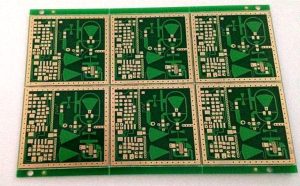
Before production, engineers should verify the electrical behavior of the PCB through appropriate simulation and testing.
Simulation may evaluate:
- Controlled impedance
- Signal reflection
- Insertion loss
- Return loss
- Crosstalk
- Electromagnetic coupling
- Thermal behavior
- Power integrity
- Antenna performance
Depending on the application, laboratory testing may include network-analyzer measurements, TDR impedance testing, dielectric characterization, electrical testing, and environmental qualification.
Simulation and measurement should be considered complementary. A well-designed simulation model helps identify potential problems before fabrication, while physical testing confirms actual PCB performance.
High-Frequency PCB Manufacturing Process
The PCB Manufacturing process for high-frequency boards requires tighter control than many conventional PCB applications.
Material properties, dimensional tolerances, copper roughness, layer registration, lamination, drilling, plating, and surface finishing can all influence RF performance.
1. PCB Design Review
The manufacturing process begins with a detailed design-for-manufacturing review.
Engineers should verify:
- Layer stack-up
- Material selection
- Controlled impedance
- Trace geometry
- Via structures
- Copper thickness
- Dielectric thickness
- Manufacturing tolerances
The design should be evaluated before fabrication to identify potential manufacturability and signal-integrity problems.
2. Inner-Layer Fabrication
The required circuit patterns are transferred to the copper layers using imaging technology.
High-frequency boards require accurate control of trace geometry because small dimensional changes can affect impedance.
3. Lamination
The prepared layers are aligned and laminated under controlled temperature and pressure.
For high-frequency materials, the lamination process must account for the material’s thermal and mechanical characteristics.
Accurate dielectric thickness and layer registration are especially important for controlled-impedance structures.
4. Drilling
Mechanical drilling and laser drilling may both be used depending on the board structure.
The drilling method is selected according to hole diameter, layer connection requirements, material characteristics, aspect ratio, and manufacturing capability.
5. Copper Plating
After drilling, the holes are prepared and copper-plated to establish electrical connections between layers.
Plating thickness and uniformity must be controlled carefully to ensure electrical and mechanical reliability.
6. Outer-Layer Processing
The outer-layer circuit patterns are formed using imaging, plating, and etching processes.
For high-frequency transmission lines, trace width and spacing must remain within the specified manufacturing tolerance.
7. Solder Mask and Surface Finish
Solder mask and surface finish are applied according to the PCB design and assembly requirements.
For RF applications, surface finish selection should also consider its influence on solderability, conductor geometry, and high-frequency electrical performance.
8. Electrical Testing and Inspection
Finished boards may undergo:
- Automated optical inspection
- Electrical continuity testing
- Insulation testing
- Dimensional inspection
- Impedance testing
- Microsection analysis
- Reliability testing
For demanding RF applications, additional electrical characterization may be required.
High-Frequency PCB Applications
RF PCB and microwave PCB technology is used across a wide range of advanced electronic systems.
Typical applications include:
- 5G communication equipment
- Wireless communication systems
- Wi-Fi equipment
- RF modules
- Radar systems
- Automotive radar
- Satellite communication
- Antenna systems
- Microwave communication
- Base stations
- Medical imaging equipment
- Aerospace electronics
- Defense electronics
- Navigation systems
- Industrial sensing equipment
- IoT communication devices
RF and Microwave Applications
A Microwave PCB is generally designed for circuits operating at microwave frequencies where transmission-line loss, impedance, dielectric properties, and electromagnetic coupling become particularly important.
Applications can include radar, satellite communication, microwave links, antennas, and advanced wireless systems.
High-Frequency PCB Industry Trends in China
China has become an important manufacturing center for advanced PCB technologies, including high-frequency, high-speed, HDI, flexible, rigid-flex, and other specialized PCB solutions.
The growth of 5G communications, automotive radar, satellite systems, data infrastructure, industrial automation, and IoT applications continues to increase demand for high-performance PCB materials and manufacturing technologies.
Common material categories used in China’s high-frequency PCB industry include:
- PTFE-based laminates
- Hydrocarbon/ceramic laminates
- Advanced FR-4 materials
- High-Tg materials
- Low-loss laminates
- Hybrid dielectric constructions
The specific material should be selected according to the frequency range, loss requirements, impedance target, thermal environment, mechanical requirements, and production process.
Why Choose Kingda for High-Frequency PCB Manufacturing?
Kingda provides PCB manufacturing solutions for customers requiring high-frequency and high-speed circuit boards.
Our engineering approach focuses on the key factors that determine high-frequency PCB performance, including:
- High-frequency material selection
- Stack-up optimization
- Controlled impedance
- Signal integrity
- Copper surface characteristics
- Precision lamination
- Mechanical and laser drilling
- Copper plating
- Layer registration
- Electrical testing
- Quality inspection
For complex RF and microwave designs, manufacturability should be considered from the earliest design stage. Close cooperation between the PCB designer and manufacturer helps ensure that material specifications, impedance requirements, dimensional tolerances, and production capabilities are properly aligned.
Conclusion
A High-Frequency PCB is designed to provide stable and reliable electrical performance when handling high-frequency signals. Compared with conventional PCB technology, it places greater emphasis on dielectric properties, copper characteristics, impedance control, transmission-line geometry, grounding, and signal integrity.
Selecting appropriate High-Frequency PCB Materials is only the first step. Successful high-frequency products also require careful High-Frequency PCB Design, accurate stack-up control, appropriate transmission-line structures, optimized via design, and tightly controlled PCB Manufacturing processes.
As demand for 5G, RF communication, automotive radar, satellite communication, wireless systems, and other advanced technologies continues to grow, high-frequency PCB technology will remain an important foundation for next-generation electronic products.