What Are Blind and Buried Via PCBs?
A Blind and Buried Via PCB is a printed circuit board that uses blind vias, buried vias, or both to establish electrical connections between different circuit layers while maximizing available board space.
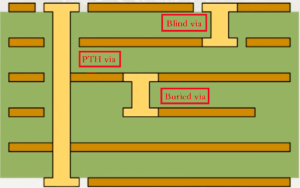
In a conventional multilayer PCB, a plated through-hole (PTH) typically extends from the top layer to the bottom layer. It passes through the entire board and is metallized to provide electrical connectivity between multiple layers.
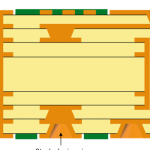
A blind via, by contrast, starts from an outer layer and terminates at one or more inner layers. Because it does not pass through the entire PCB, the via is visible from only one side of the board.
A buried via is completely located within the inner layers of the PCB. Both ends of the via are connected to internal layers, so it cannot be seen from the external surfaces after the PCB has been laminated.
For example, in a six-layer PCB:
- L1–L2 or L1–L3 connections can be implemented using blind vias.
- L2–L3, L2–L4, or L3–L4 connections can be implemented using buried vias.
- L1–L6 can use a conventional plated through-hole.
Because blind and buried vias reduce the amount of board surface occupied by through-holes, they are widely used in HDI PCB designs and other high-density electronic products.
Why Are Blind and Buried Vias Needed?
The development of blind and buried vias is closely related to the increasing complexity and miniaturization of electronic products.
Traditional multilayer PCBs rely heavily on through-holes to connect different circuit layers. Although through-holes are relatively simple to manufacture, they extend through the entire board and occupy valuable routing space on every layer they pass through.
As electronic products become smaller, designers need to place more components and routing channels within the same PCB area. At the same time, component packages have become smaller and interconnection densities have increased.
This creates several challenges:
- More signal connections must fit into a limited PCB area.
- Fine-pitch components require higher routing density.
- High-speed interfaces require carefully controlled signal paths.
- Through-holes can consume valuable routing channels.
- Large numbers of through-holes can complicate signal and power distribution.
- Smaller products require more efficient use of every PCB layer.
Blind and buried vias address these limitations by allowing designers to connect only the layers that actually need to be connected.
Instead of routing a connection through the entire PCB, a designer can use a blind or buried via to create a shorter and more localized interconnection.
When Did Blind and Buried Via Technology Emerge?
Blind and buried via technology became increasingly important as the PCB and electronics industries moved toward higher density and greater miniaturization during the late 20th and early 21st centuries.
The rapid development of mobile communications, computers, portable electronics, networking equipment, and other compact electronic products created strong demand for smaller and more densely interconnected PCBs.
PCB technology consequently evolved from conventional single- and double-sided boards toward:
- Multilayer PCBs
- HDI PCBs
- Flexible PCBs
- Rigid-flex PCBs
- Blind via PCBs
- Buried via PCBs
- Microvia-based PCB structures
These technologies allow manufacturers to increase interconnection density without simply increasing PCB dimensions.
What Is a Buried Via?
A Buried Via PCB uses vias that are located entirely between internal PCB layers.
Unlike a through-hole, a buried via does not extend to the external surface. Unlike a blind via, it does not begin or end on an external layer.
For example, in a six-layer PCB, connections such as L2–L3, L2–L4, L2–L5, L3–L4, and L3–L5 can be implemented using buried vias when supported by the stack-up and manufacturing process.
The key characteristics of buried vias include:
- Located entirely within the PCB
- Connect two or more internal layers
- Do not occupy routing space on the external layers
- Improve internal layer utilization
- Suitable for high-density multilayer designs
- Require controlled manufacturing processes
How Are Buried Vias Manufactured?
Buried vias generally require a sequential manufacturing process rather than simply drilling the completed PCB.
A typical process may involve:
- Fabricating selected inner-layer cores.
- Drilling the required via holes.
- Plating the holes to establish electrical connections.
- Laminating the processed subassembly with additional dielectric and copper layers.
- Completing the remaining PCB fabrication processes.
Because some buried vias must be fabricated before the entire multilayer structure is laminated, process planning and layer registration become especially important.
This additional processing increases manufacturing complexity and cost compared with conventional through-hole PCBs.
What Is a Blind Via?
A Blind Via PCB uses vias that connect an external copper layer to one or more internal layers without passing completely through the board.
A blind via can start from either the top or bottom surface.
For example, in a six-layer PCB:
- L1–L2 can use a top-side blind via.
- L1–L3 can use a deeper blind via.
- L6–L5 can use a bottom-side blind via.
- L6–L4 can also be implemented using a bottom-side blind via.
The exact allowable blind-via depth depends on the PCB stack-up, aspect ratio, drilling method, dielectric thickness, and manufacturing capability.
Advantages of Blind Vias
Blind vias provide several important advantages for high-density PCB design:
- Save routing space on external layers.
- Reduce unnecessary through-hole structures.
- Increase component and routing density.
- Support fine-pitch component escape routing.
- Provide more flexible multilayer interconnections.
- Help optimize compact PCB layouts.
- Can improve high-speed signal routing when properly designed.
Blind vias are particularly valuable around BGA, CSP, QFN, and other fine-pitch packages where conventional through-holes may consume too much routing space.
Blind Vias, Buried Vias, and Through-Holes Compared
Understanding the difference between these three via structures is essential for selecting the correct PCB technology.
| Via Type | Connection | External Visibility | Typical Application |
|---|---|---|---|
| Through-Hole Via | Top to bottom | Visible on both sides | Conventional multilayer PCBs |
| Blind Via | Outer layer to inner layer | Visible from one side | HDI and high-density designs |
| Buried Via | Inner layer to inner layer | Not externally visible | High-density multilayer PCBs |
A combination of these structures can be used within the same PCB when required.
For example, an advanced HDI board may use through-holes for major layer-to-layer connections, blind microvias for outer-layer routing, and buried vias for internal connections.
What Is a Microvia PCB?
Many blind and buried via structures use very small via diameters. These structures are commonly associated with Microvia PCB technology.
Microvias are generally manufactured using laser drilling rather than conventional mechanical drilling. Their small dimensions allow designers to create more compact interconnections and route signals through areas that would be difficult to access with conventional vias.
Microvias are particularly common in HDI PCB manufacturing and are frequently used for:
- BGA escape routing
- Fine-pitch component interconnections
- High-density mobile electronics
- Compact communication equipment
- High-speed digital systems
- Miniaturized consumer electronics
The actual microvia diameter and aspect ratio depend on the material system, PCB stack-up, laser system, and manufacturer’s process capability.
Laser Drilling for Blind and Buried Vias
Modern Laser Drilling technology plays an important role in the production of HDI and microvia PCBs.
Traditional mechanical drilling can be used for certain blind-via structures, particularly when the required depth and hole diameter are relatively large. However, laser drilling provides greater flexibility for very small microvias and controlled-depth structures.
Common laser technologies used in PCB fabrication include:
- CO₂ laser
- UV/YAG laser
- Excimer laser
Different laser wavelengths interact differently with copper and dielectric materials. Therefore, the choice of laser system depends on the PCB material, copper thickness, hole diameter, dielectric structure, and required production volume.
Why Is Laser Drilling Important?
Laser drilling offers several advantages for advanced PCB manufacturing:
- Very small hole diameters
- Precise depth control
- High drilling density
- Suitable for microvia structures
- Efficient processing of high-density interconnections
- Reduced dependence on conventional mechanical drilling
For example, laser drilling can be used to form microvias between an outer copper layer and the adjacent dielectric layer, creating compact interconnections for HDI designs.
Manufacturing Challenges of Blind and Buried Via PCBs
Although blind and buried vias provide major design advantages, they also make PCB Manufacturing more complicated.
Layer Registration
Multiple lamination and drilling processes require highly accurate layer-to-layer registration.
Small alignment errors can cause via misregistration, reducing the available capture pad area or even creating open circuits.
Drilling Accuracy
Blind and microvia structures require precise control of hole diameter and depth.
The drilling process must be compatible with the dielectric thickness and copper structure. Excessive drilling depth or insufficient depth can both lead to reliability problems.
Copper Plating
Reliable copper plating is essential for establishing a continuous electrical connection inside the via.
For microvias, plating must adequately cover the hole wall and provide sufficient mechanical and electrical reliability.
Lamination Control
Buried-via structures may require sequential lamination. This introduces additional requirements for:
- Material selection
- Resin flow
- Layer alignment
- Lamination temperature
- Lamination pressure
- Dimensional stability
Reliability Testing
Advanced via structures should be evaluated for reliability under the expected operating conditions.
Depending on the application, testing may include electrical continuity, insulation resistance, thermal cycling, microsection analysis, solderability, and other qualification tests.
Design Considerations for Blind and Buried Via PCBs
Before designing a Blind and Buried Via PCB, engineers should work closely with the PCB manufacturer to define realistic design rules.
Important considerations include:
- PCB layer count
- Stack-up structure
- Via diameter
- Via depth
- Aspect ratio
- Capture pad size
- Land diameter
- Via-to-via spacing
- Via-to-trace clearance
- Dielectric thickness
- Copper thickness
- Laser drilling capability
- Mechanical drilling capability
- Sequential lamination requirements
- Registration tolerance
- Surface finish
- Electrical and reliability requirements
Designers should avoid selecting unnecessarily small vias or extremely tight tolerances unless the application requires them. A manufacturable design can reduce production risk and improve overall cost efficiency.
Applications of Blind and Buried Via PCBs
Blind and buried via technology is widely used where PCB size, routing density, and electrical performance are critical.
Typical applications include:
- Smartphones and mobile devices
- Wearable electronics
- High-performance computers
- Networking equipment
- 5G communication systems
- Automotive electronics
- Medical devices
- Industrial control systems
- Aerospace electronics
- High-speed digital equipment
- Consumer electronics
- Compact IoT devices
In particular, HDI technology enables designers to accommodate more interconnections within smaller PCB footprints, making blind and buried vias especially valuable for miniaturized electronic products.
Blind and Buried Via PCB vs. Conventional Multilayer PCB
The primary difference is how interlayer connections are distributed.
A conventional multilayer PCB often relies heavily on through-holes. These holes pass through multiple layers, even when only two specific layers need to be connected.
A blind and buried via design allows the connection to be localized.
For example, if a signal only needs to travel from L1 to L2, a blind via can be used instead of a through-hole. If a connection is required only between L3 and L4, a buried via can perform the connection internally.
This approach frees routing space on other layers and enables more efficient use of the PCB’s available area.
Why Choose Kingda for Blind and Buried Via PCB Manufacturing?
As PCB designs continue to become smaller, faster, and more complex, blind and buried via technology is increasingly important for advanced electronic products.
Kingda provides PCB manufacturing solutions for high-density multilayer and HDI applications, including boards incorporating blind vias, buried vias, microvias, and other advanced interconnection structures.
Our manufacturing process focuses on critical factors such as:
- Material selection
- Stack-up optimization
- Laser drilling
- Mechanical drilling
- Copper plating
- Sequential lamination
- Layer registration
- Electrical testing
- Dimensional inspection
- PCB reliability
By considering manufacturability during the design stage, engineers can achieve a better balance between PCB density, electrical performance, reliability, production yield, and cost.
Conclusion
Blind and buried vias are important technologies for modern high-density PCB design. A Blind Via PCB connects an external layer to one or more internal layers, while a Buried Via PCB connects internal layers without reaching the external surfaces.
When combined with microvias and laser drilling, these technologies can significantly improve routing density and make better use of limited PCB space.
Although blind and buried via structures require more sophisticated PCB Manufacturing processes than conventional through-holes, they provide substantial advantages for compact, high-performance electronic systems.
For demanding HDI and multilayer applications, selecting the appropriate via structure, stack-up, material, drilling method, and manufacturing process is essential to achieving reliable and cost-effective PCB production.