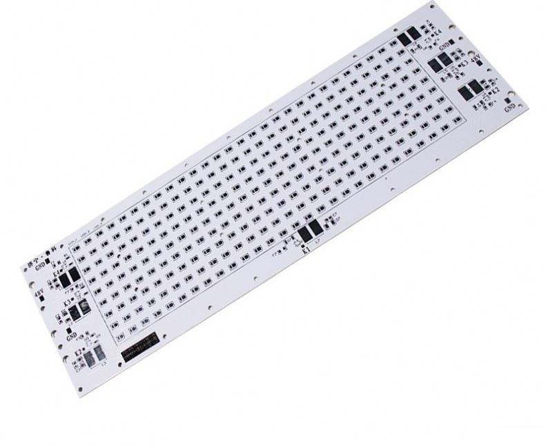
LED PCB: PCB Design, PCB Manufacturing, Materials, Applications & Thermal Management Guide
Lighting has become an essential part of modern life. From indoor residential lighting to outdoor infrastructure, industrial facilities, automotive systems, and specialized equipment, lighting technology plays an important role in everyday activities and industrial operations.
The lighting industry has undergone several major technological transformations. Among them, LED (light-emitting diode) technology has become one of the most widely adopted solutions because of its efficiency, long service life, compact size, controllability, and design flexibility.
As demand continues to grow for lower energy consumption, longer operating life, improved reliability, and environmentally conscious products, LED PCB technology has become increasingly important. LED circuit boards provide the electrical interconnection, mechanical support, and thermal-management foundation required by LED lighting systems.
However, designing and manufacturing an LED PCB involves more than simply placing LEDs on a circuit board. Engineers must consider LED driver design, current distribution, component placement, thermal resistance, PCB materials, optical requirements, manufacturing tolerances, and assembly reliability.
This guide explains what an LED PCB is, how to approach LED PCB Design, which materials are commonly used, how LED PCBs are manufactured, and where they are used.
What Is an LED PCB?
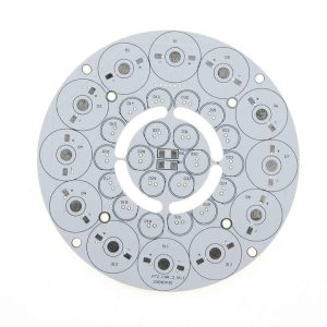
An LED PCB is a printed circuit board specifically designed to electrically and mechanically support LEDs and their associated components.
LED PCBs are commonly used in:
- General lighting
- LED indicators
- Automotive lighting
- Display systems
- Industrial equipment
- Consumer electronics
- Medical equipment
- Aerospace and defense systems
- Architectural lighting
- Outdoor lighting
An LED is a semiconductor device that emits light when current flows through it under appropriate operating conditions. The amount of light, color, efficiency, and operating temperature depend on the LED technology and the electrical conditions applied to it.
The PCB provides the conductive paths needed to distribute electrical power and signals to the LEDs. It can also provide a thermal path for transferring heat away from LED packages.
For high-power lighting systems, thermal performance can be just as important as electrical performance. Excessive junction temperature can reduce LED efficiency, accelerate aging, and shorten operating life.
LED PCB Design Considerations
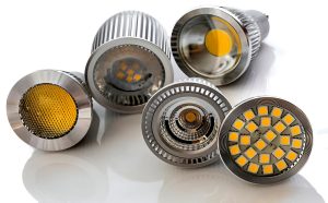
Designing an LED circuit board requires coordination between electrical, mechanical, optical, and thermal requirements.
The major considerations include:
- LED driver design
- LED load configuration
- Current distribution
- Component placement
- Thermal management
- PCB material selection
- Board dimensions
- Optical arrangement
- Assembly requirements
- Reliability requirements
1. LED Driver Circuit Design
An LED system typically consists of two major functional sections:
- LED driver
- LED load
The LED driver supplies the electrical power required by the LED load.
Unlike some conventional electronic loads, LEDs can be sensitive to current variations. Depending on the architecture, LED systems may therefore use constant-current or constant-voltage driver configurations.
The appropriate driver depends on the LED configuration and system requirements.
An LED driver may provide functions such as:
- Constant-current regulation
- Dimming control
- Overvoltage protection
- Overcurrent protection
- Surge protection
- Short-circuit protection
- Thermal protection
- Power-factor correction in applicable systems
- High conversion efficiency
For high-power lighting, driver efficiency is particularly important because electrical losses are converted into heat.
A poorly designed driver can therefore increase both electrical consumption and thermal stress.
2. LED Load Circuit Design
The LED load circuit contains the LED array responsible for producing the required optical output.
LED packages are available in many configurations, allowing designers to optimize:
- Brightness
- Color temperature
- Wavelength
- Beam characteristics
- Power level
- Package size
- Optical distribution
The LED array should be designed according to the required electrical and optical performance.
For example, LEDs may be connected in series, parallel, or a combination of both depending on the driver architecture and system requirements.
Current balancing becomes particularly important in parallel LED configurations because differences in forward voltage can cause uneven current distribution.
Therefore, the electrical architecture should be evaluated together with the selected LED specifications.
3. LED PCB Layout Preparation
After the schematic and electrical architecture have been completed, the design is converted into a physical PCB layout.
The layout should consider:
- LED spacing
- Driver component placement
- Power routing
- Grounding
- Thermal paths
- Mechanical mounting
- Connector locations
- Optical requirements
- Manufacturing constraints
LEDs may need to be distributed evenly across the board to achieve consistent illumination.
For larger LED arrays, the physical layout must also consider voltage drop and current distribution so that LEDs located at different positions receive appropriate electrical power.
High-current traces should be sufficiently wide to reduce resistance and temperature rise.
4. LED Component Placement
Component placement directly affects both electrical performance and thermal behavior.
LEDs should be positioned according to the required optical pattern, while driver components and power components should be arranged to minimize unnecessary electrical losses and thermal coupling.
For high-power LED systems, components generating significant heat should be separated from temperature-sensitive devices whenever possible.
Thermal structures may include:
- Copper thermal pads
- Thermal vias
- Large copper areas
- Metal-core PCB structures
- Heat sinks
- Thermal interface materials
The final structure should provide a controlled thermal path from the LED junction toward the surrounding environment.
LED PCB Materials
Material selection is a critical part of PCB Manufacturing because the PCB material directly affects electrical insulation, mechanical strength, thermal performance, reliability, and cost.
Common LED PCB material options include:
- FR-4
- Aluminum-based PCB materials
- Copper-based metal-core structures
- Ceramic substrates
The appropriate material depends on the application’s power density, thermal requirements, operating environment, mechanical structure, and cost target.
FR-4 LED PCBs
FR-4 is widely used because it provides:
- Good mechanical strength
- Reliable electrical insulation
- Broad manufacturing availability
- Relatively low cost
- Compatibility with conventional PCB fabrication and assembly
FR-4 can be suitable for low- and moderate-power LED applications where thermal requirements are manageable.
However, its thermal conductivity is generally much lower than that of metal-core or ceramic solutions.
Aluminum LED PCBs
Aluminum-based PCBs are widely used in LED lighting because they provide an efficient thermal path.
A typical metal-core LED PCB includes:
- Copper circuit layer
- Dielectric insulation layer
- Aluminum metal core
The aluminum core spreads heat away from high-temperature areas and toward a heat sink or chassis.
This structure can be particularly useful for:
- High-power LED lighting
- Street lighting
- Automotive lighting
- Industrial lighting
- Floodlights
- Architectural lighting
Copper and Ceramic Materials
Copper-based structures can provide excellent thermal conductivity and are useful for applications with demanding thermal requirements.
Ceramic substrates can also provide high thermal performance combined with strong electrical insulation and good dimensional stability.
However, these materials may involve higher manufacturing costs and different fabrication requirements compared with conventional FR-4.
Material selection should therefore be based on the complete system rather than thermal conductivity alone.
LED PCB Manufacturing Process
The LED PCB Manufacturing process is broadly similar to conventional PCB fabrication, although LED applications may require additional thermal and dimensional considerations.
A typical manufacturing workflow includes the following steps.
1. PCB Design and Engineering Review
The process begins with schematic development and PCB layout.
The design package may include:
- Schematic files
- PCB layout files
- Gerber files
- Drill files
- Bill of materials (BOM)
- Assembly drawings
- Pick-and-place data
- Manufacturing specifications
Before fabrication, the design should undergo DFM and assembly reviews.
The manufacturer can identify issues involving:
- Trace width
- Spacing
- Via structures
- Copper thickness
- Thermal pads
- Component footprints
- Board dimensions
- Assembly clearances
2. Material Preparation and Lamination
The PCB material is selected according to the design requirements.
For multilayer LED PCBs, the required copper layers and dielectric materials are stacked according to the specified stackup.
The stackup must maintain the required electrical insulation and mechanical structure.
For metal-core LED PCBs, the dielectric layer must provide both electrical isolation and an effective thermal path.
3. Drilling and Circuit Formation
Depending on the PCB structure, holes are drilled for through-hole components and vias.
The circuit pattern is then transferred to the copper surface and unwanted copper is removed through controlled etching.
For high-current LED applications, copper thickness should be selected according to current requirements and thermal considerations.
4. Copper Plating
For PCBs requiring plated through-holes or vias, copper plating creates electrical connections between conductive layers.
The plating process must provide reliable electrical and mechanical connections.
For multilayer boards, reliable via structures are particularly important because they may also contribute to thermal transfer.
5. Solder Mask and Surface Finish
A solder mask is applied to protect exposed copper areas and reduce the risk of solder bridging and environmental contamination.
The PCB then receives an appropriate surface finish, depending on the assembly technology and product requirements.
Potential finishes include:
- HASL
- Lead-free HASL
- ENIG
- OSP
- Immersion tin
- Immersion silver
The correct surface finish depends on component pitch, assembly process, storage requirements, reliability expectations, and cost.
6. LED PCB Assembly
After bare-board fabrication, LED components and supporting electronics can be assembled onto the PCB.
Depending on the design, assembly may use:
- SMT
- Through-hole technology (THT)
- Reflow soldering
- Selective soldering
- Manual assembly for prototypes or special applications
LED placement accuracy is particularly important when the PCB is part of an optical system.
For high-density LED arrays, placement tolerances can affect both electrical consistency and optical uniformity.
7. LED PCB Testing
Testing is essential for verifying electrical performance and manufacturing quality.
Typical inspection and testing may include:
- Visual inspection
- AOI
- Electrical continuity testing
- Insulation testing where applicable
- Functional testing
- LED brightness verification
- Color or optical testing
- Thermal testing
- Assembly inspection
For high-power LED products, thermal testing can be especially valuable because electrical performance alone does not guarantee long-term reliability.
LED PCB Thermal Management
Thermal management is one of the most important considerations in high-power LED applications.
Although LEDs are more energy-efficient than many older lighting technologies, not all electrical input power is converted into visible light. The remaining energy contributes to heat generation.
If heat cannot be effectively removed, LED junction temperature can increase.
Excessive temperature can result in:
- Reduced luminous efficiency
- Color shift
- Accelerated degradation
- Reduced service life
- PCB reliability problems
- Component failure
Therefore, thermal design should begin during the initial PCB Design stage.
Thermal Vias
Thermal vias can transfer heat from an LED pad into internal or bottom copper structures.
Copper Spreading
Large copper areas can distribute heat over a larger surface area.
Metal-Core PCB
Metal-core PCBs provide a low-resistance thermal path compared with conventional FR-4 structures.
Heat Sinks
Heat sinks can transfer heat from the PCB or component assembly into the surrounding environment.
Thermal Interface Materials
Thermal pads and thermal interface materials can improve heat transfer between the PCB and an external heat sink or chassis.
The complete thermal path should be considered:
LED Junction → Package → PCB → Thermal Interface → Heat Sink → Environment
Optimizing only one part of this path may not provide sufficient thermal performance.
LED PCB Applications
LED PCBs are used across a wide range of industries because of the efficiency, compactness, controllability, and long operating life of LED technology.
1. Consumer Electronics
LED PCBs are widely used in consumer electronics for:
- Display backlighting
- Status indicators
- Keypad illumination
- Television displays
- Computer monitors
- Consumer appliances
In these applications, compact size and low power consumption are often important design requirements.
2. Industrial Lighting
Industrial applications include:
- Factory lighting
- Machine indicators
- Control-panel illumination
- Warehouse lighting
- Industrial inspection systems
- High-bay lighting
Industrial LED PCBs often require higher reliability because equipment may operate for extended periods and under demanding environmental conditions.
3. Automotive Lighting
LED PCBs are increasingly used in automotive systems, including:
- Headlamps
- Tail lamps
- Brake lights
- Turn indicators
- Interior lighting
- Dashboard illumination
- Ambient lighting
Automotive LED PCB design must account for vibration, temperature cycling, electrical transients, moisture, and long-term reliability.
4. Medical Equipment
LED technology is used in medical and healthcare equipment where controlled illumination is required.
Applications can include:
- Surgical lighting
- Examination equipment
- Diagnostic instruments
- Medical indicators
- Optical instruments
Medical LED PCB designs may require stringent reliability, thermal, cleanliness, and regulatory considerations depending on the equipment.
5. Telecommunications and Networking Equipment
LED indicators are commonly used to communicate equipment status, link activity, power conditions, and fault information.
Although the LEDs themselves may consume relatively little power, the PCB must still provide reliable electrical connections and appropriate indicator control.
6. Aerospace and Defense
Aerospace and defense systems may use LED PCBs for:
- Cockpit indicators
- Instrument illumination
- Display systems
- Navigation-related indicators
- Interior lighting
- Specialized equipment
These applications may require lightweight construction, high reliability, thermal stability, and resistance to demanding environmental conditions.
Advantages of LED PCB Technology
LED PCB technology provides several important benefits.
Energy Efficiency
LED systems can provide high luminous efficiency while consuming less electrical power than many conventional lighting technologies.
Long Service Life
Properly designed LED systems can provide long operating life, particularly when junction temperature and electrical stress are well controlled.
Compact Design
LED packages and PCBs allow designers to create compact lighting modules.
Design Flexibility
LED arrays can be arranged to produce different colors, brightness levels, optical patterns, and lighting geometries.
Thermal Optimization
Metal-core and ceramic PCB technologies can provide improved thermal management for demanding applications.
Intelligent Lighting Integration
Modern LED PCBs can be combined with sensors, wireless communication, microcontrollers, and dimming systems to support smart lighting functions.
Common LED PCB Design Challenges
Despite their advantages, LED PCBs can present several engineering challenges.
1. Uneven Current Distribution
Parallel LED configurations may experience current imbalance if the electrical design is not carefully controlled.
2. Excessive Temperature
Insufficient thermal management can reduce LED efficiency and operating life.
3. Voltage Drop
Long or undersized power traces can cause voltage differences across an LED array.
4. Poor Component Placement
Improper placement can create thermal hotspots or interfere with optical uniformity.
5. Driver Compatibility
The LED driver must match the electrical characteristics of the LED load.
6. Manufacturing Variation
Variations in PCB thickness, copper distribution, component placement, and soldering can affect electrical and thermal performance.
How to Improve LED PCB Design and Manufacturing
A reliable LED PCB development process should include:
- Define the required optical output.
- Determine LED electrical characteristics.
- Select the appropriate LED driver.
- Determine current and voltage requirements.
- Select the PCB material.
- Develop the LED array configuration.
- Optimize component placement.
- Design current and power distribution.
- Analyze thermal performance.
- Add thermal vias or metal-core structures where required.
- Complete DFM and DFA reviews.
- Manufacture a prototype.
- Test electrical and thermal performance.
- Validate optical performance.
- Optimize the design before volume production.
This integrated approach helps ensure that electrical, optical, thermal, and manufacturing requirements are considered simultaneously.
LED PCB Design and Manufacturing with Kingda
For LED lighting products, selecting an experienced PCB manufacturing partner can help reduce development risks and improve production consistency.
Kingda provides PCB fabrication and PCBA services that can support prototype development and production applications.
Depending on project requirements, Kingda can support areas such as:
- PCB design review
- DFM/DFA analysis
- FR-4 PCB fabrication
- Metal-core PCB solutions
- Multilayer PCB manufacturing
- SMT assembly
- THT assembly
- Reflow soldering
- AOI inspection
- X-ray inspection
- Electrical testing
- Functional testing
- Final assembly
Early collaboration with the manufacturing team can help engineers evaluate material selection, copper thickness, thermal structures, component footprints, assembly requirements, and manufacturing tolerances before production begins.
Conclusion
LED technology has transformed the lighting industry by providing efficient, compact, controllable, and long-lasting lighting solutions.
At the center of many of these systems is the LED PCB, which provides electrical connectivity, mechanical support, and, in many applications, an important thermal path.
Successful LED PCB Design requires careful consideration of LED driver circuits, LED array configuration, current distribution, component placement, thermal management, material selection, optical requirements, and manufacturability.
At the same time, reliable PCB Manufacturing requires appropriate fabrication processes, material control, surface finishing, assembly accuracy, inspection, and electrical and thermal testing.
For low- and moderate-power applications, FR-4 may provide a cost-effective solution. For high-power lighting, metal-core or ceramic PCB technologies may offer better thermal performance.
As smart lighting, automotive electronics, industrial automation, medical equipment, and energy-efficient systems continue to expand, LED PCB technology will remain an important part of next-generation electronic products.
Article Summary
An LED PCB is a circuit board designed specifically to support LEDs and their associated electronic components. It provides electrical connections, mechanical support, and, depending on the PCB structure, an important path for heat dissipation.
The key elements of LED PCB Design include LED driver selection, LED array configuration, current distribution, component placement, thermal management, PCB material selection, and manufacturing considerations.
During PCB Manufacturing, processes such as circuit formation, drilling, plating, solder-mask application, surface finishing, SMT assembly, inspection, and electrical testing must be carefully controlled.
For demanding high-power LED applications, aluminum metal-core PCBs and ceramic substrates can provide improved thermal performance, while FR-4 remains a practical choice for many lower-power applications.
Overall, the combination of appropriate PCB materials, efficient thermal management, optimized circuit design, and controlled manufacturing processes is essential for developing reliable, efficient, and long-lasting LED products.