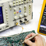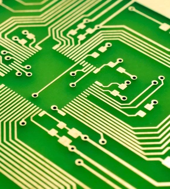
PCB Manufacturing is the process of converting a PCB design into a physical, functional printed circuit board. It involves a series of controlled manufacturing operations that create conductive patterns, dielectric structures, plated interconnections, protective coatings, and finished surface features on a PCB.
A printed circuit board provides both mechanical support and electrical interconnection for electronic components. Depending on the application, PCB structures can range from simple single-sided boards to complex multilayer, flexible, rigid-flex, HDI, high-frequency, and metal-based circuit boards.
The exact PCB Manufacturing Process depends on the board structure, material system, layer count, feature dimensions, copper thickness, via technology, surface finish, and performance requirements. A typical process may include material preparation, inner-layer imaging, etching, lamination, drilling, desmear, copper plating, outer-layer imaging, solder mask, surface finish, silkscreen, routing, inspection, and electrical testing.
It is important to distinguish PCB Fabrication from PCB assembly. PCB fabrication produces the bare circuit board, while PCB assembly involves mounting and soldering electronic components onto the finished PCB.
PCB Manufacturing Capabilities
A PCB manufacturer may support a wide range of board technologies depending on its equipment, process control, and engineering capabilities.
Typical PCB structures include:
- Rigid PCB
- Flexible PCB
- Rigid-Flex PCB
- Semi-flexible PCB
- HDI PCB
- RF and microwave PCB
- IC substrates
- High-speed PCB
- High-frequency PCB
- Metal-core PCB
- Ceramic PCB
Common material systems include:
- FR-4
- Polyimide
- PET
- Aluminum
- Copper
- Metal-core materials
- Alumina ceramic
- High-frequency laminates
- PTFE-based materials
- Halogen-free materials
- Mixed-material constructions
Advanced PCB technologies may include:
- Blind vias
- Buried vias
- Microvias
- Via-in-pad
- Conductive via filling
- Non-conductive via filling
- Back drilling
- Controlled impedance
- Heavy copper
- Gold fingers
- Embedded components
- Fine-line circuitry
Board thickness, layer count, panel dimensions, and other manufacturing capabilities vary by manufacturer and technology. Therefore, actual capabilities should always be confirmed against the supplier’s current process specifications before design release.
What Is PCB Manufacturing?
The primary purpose of PCB manufacturing is to create reliable electrical connections while providing mechanical support for electronic components.
A typical PCB consists of several fundamental elements:
- Conductive copper layers
- Dielectric insulating materials
- Copper-plated vias
- Solder mask
- Surface finish
- Silkscreen or other marking layers
For a standard rigid PCB, FR-4 is one of the most widely used dielectric material systems. However, high-speed, RF, thermal, flexible, automotive, aerospace, and other demanding applications may require specialized materials.
PCB manufacturing connects the electrical design defined by the engineering team with a physical board that can be assembled and tested.
A Brief History of PCB Manufacturing
The development of PCB technology has closely followed the evolution of electronic devices.
Early Printed Wiring Concepts
Early printed wiring concepts emerged during the first decades of the 20th century. Engineers explored methods for creating conductive paths on insulating substrates instead of using extensive point-to-point wiring.
Development of Practical PCBs
During the 1930s, practical printed circuit construction became increasingly important. Printed wiring techniques were applied to electronic equipment and gradually developed into the PCB technologies used today.
Postwar Electronics Development
After World War II, advances in electronics, telecommunications, and semiconductor technology increased the need for more compact and repeatable circuit interconnections.
Multilayer PCB Development
The growth of computers, aerospace systems, and increasingly complex electronics drove the development of multilayer PCB structures. Additional conductive and dielectric layers allowed designers to achieve greater routing density within a smaller footprint.
Surface Mount Technology
The development of surface mount technology further reduced component size and enabled higher assembly density. PCB manufacturing processes evolved to support smaller pads, finer traces, tighter tolerances, and improved surface finishes.
Modern Electronics
The growth of smartphones, wireless communication, cloud computing, IoT, automotive electronics, and advanced computing has continued to increase PCB complexity.
Today, PCB manufacturing is increasingly influenced by miniaturization, high-speed data transmission, advanced packaging, thermal management, high-density interconnects, and sustainability.
Common Types of PCBs
PCBs can be classified according to layer count, mechanical structure, material, application, or manufacturing technology.
The most common classifications include single-sided, double-sided, multilayer, rigid, flexible, and rigid-flex PCBs.
Single-Sided PCB
A single-sided PCB contains one primary conductive copper layer. Components are generally mounted on one side, while conductive traces are formed on the copper layer.
Because its structure is relatively simple, a single-sided PCB can be suitable for cost-sensitive products with limited circuit density.
Typical applications include:
- Basic control circuits
- LED products
- Simple consumer electronics
- Power-related devices
- Industrial control boards
Double-Sided PCB
A double-sided PCB contains conductive copper layers on both sides of the dielectric substrate.
Plated through-holes can electrically connect the top and bottom layers, allowing routing density to be significantly increased compared with single-sided boards.
Double-sided PCBs are widely used in:
- Industrial electronics
- Consumer products
- Power supplies
- Control systems
- Instrumentation
Multilayer PCB
A Multilayer PCB contains three or more conductive layers separated by dielectric materials.
Internal layers can be dedicated to signal routing, power distribution, ground planes, or other electrical functions. Vias and microvias provide vertical interconnections between different layers.
A multilayer structure can provide:
- Higher routing density
- Better power and ground distribution
- Improved signal integrity
- Reduced electromagnetic coupling when properly designed
- More compact product dimensions
The multilayer manufacturing process generally involves fabricating individual inner-layer circuits, aligning and laminating the layers, drilling and plating interconnections, and completing the outer-layer processes.
Rigid PCB
A rigid PCB uses a mechanically stable substrate that is not intended to flex during normal operation.
FR-4 is widely used for rigid PCBs, while metal-core and ceramic materials may be selected for applications requiring enhanced thermal performance or specialized electrical characteristics.
Rigid PCBs are commonly used in:
- Industrial equipment
- Computers
- Automotive electronics
- Telecommunications
- Medical electronics
- Consumer electronics
- Power electronics
Flexible PCB
A flexible PCB uses a bendable substrate, commonly polyimide, to enable electrical connections in applications where conventional rigid boards are difficult to install.
Flexible PCBs can reduce wiring space and support product miniaturization. They are commonly used in:
- Cameras
- Mobile devices
- Wearable electronics
- Medical devices
- Automotive electronics
- Sensors
During assembly, flexible circuits may require carriers or fixtures to maintain flatness and dimensional stability during solder paste printing and reflow.
Rigid-Flex PCB
A rigid-flex PCB combines rigid circuit sections with flexible circuit sections within a single integrated structure.
The rigid areas can provide mechanical support and component mounting, while the flexible sections can route signals between different rigid sections without requiring separate cables or connectors.
Rigid-flex PCBs are used in applications such as:
- Portable electronics
- Cameras
- Robotics
- Aerospace equipment
- Medical devices
- Automotive electronics
Polyimide is commonly used in the flexible sections because of its flexibility and thermal performance.
Applications of PCB Manufacturing
PCBs are used throughout modern electronics, including industrial automation, medical equipment, automotive systems, telecommunications, robotics, energy systems, consumer electronics, aerospace, and test equipment.
Consumer Electronics
Consumer electronics are major users of PCB technology. Smartphones, tablets, computers, televisions, cameras, wearable devices, and smart home products all require increasingly compact and high-density circuit boards.
Miniaturization and multifunctional integration continue to drive demand for finer traces, smaller vias, higher layer counts, and advanced substrate technologies.
Automation and Industrial Control
Industrial automation systems use PCBs for controllers, sensors, motor drives, communication modules, human-machine interfaces, and industrial computers.
Depending on the system requirements, these products may use multilayer or HDI PCB structures to accommodate dense circuitry and high-speed interfaces.
Industrial PCBs may also need to withstand vibration, temperature changes, dust, humidity, and extended operating periods.
Power and Energy
Power electronics rely on PCBs for power conversion, control, protection, and monitoring.
Applications include:
- Power supplies
- UPS systems
- Solar inverters
- Battery management systems
- Energy storage equipment
- Electric vehicle systems
- Charging equipment
High-current applications may require thicker copper, enhanced thermal management, larger conductor widths, and appropriate dielectric materials.
Material selection should be based on actual temperature, electrical, mechanical, and reliability requirements rather than using a single material specification for every power application.
Automotive Electronics
Automotive electronics require careful control of electrical performance, mechanical reliability, thermal behavior, and environmental durability.
PCBs are used in:
- Engine control systems
- ADAS
- Automotive cameras
- Infotainment
- Battery management
- Vehicle networking
- Sensors
- Lighting systems
- Safety-related electronics
Depending on the application, automotive PCBs may need to address vibration, thermal cycling, humidity, electromagnetic compatibility, and electrical transients.
Medical Electronics
Medical devices use PCBs for sensing, monitoring, control, communication, power management, and data processing.
Examples include:
- Patient monitoring equipment
- Diagnostic equipment
- Portable medical devices
- Imaging systems
- Laboratory equipment
- Therapeutic equipment
Medical applications require careful consideration of reliability, traceability, risk management, regulatory requirements, and intended use.
Basic Materials Used in PCB Manufacturing
Understanding PCB materials is essential because material selection affects electrical, mechanical, thermal, and manufacturing performance.
Dielectric Substrate
The dielectric material separates conductive copper layers and provides electrical insulation and mechanical support.
FR-4 is widely used in conventional rigid PCBs because it provides a practical combination of mechanical strength, electrical performance, thermal characteristics, and cost.
Specialized applications may require:
- High-Tg laminates
- Low-loss materials
- PTFE-based materials
- Polyimide
- Metal-core materials
- Ceramic substrates
- Halogen-free laminates
Core Material
A PCB core is a dielectric material with copper foil laminated to one or both sides.
In multilayer boards, cores become part of the final layer structure and determine important electrical and mechanical characteristics.
Prepreg
Prepreg is a resin-impregnated glass-fiber material used to bond PCB layers during multilayer lamination.
During the lamination cycle, heat and pressure cause the resin to flow and cure, bonding the individual layers into a consolidated multilayer structure.
Prepreg selection influences:
- Dielectric thickness
- Resin content
- Impedance
- Layer spacing
- Mechanical characteristics
- Lamination behavior
Copper Foil
Copper foil forms the conductive foundation of a PCB.
During fabrication, portions of the copper are selectively removed through imaging and etching processes to create the required circuit pattern.
Copper thickness is selected according to current-carrying requirements, signal performance, mechanical considerations, and manufacturing capability.
Solder Mask
Solder mask is a protective polymer coating applied over selected PCB surfaces.
Its functions include:
- Protecting copper from environmental exposure
- Reducing the risk of unintended solder bridging
- Providing electrical insulation between exposed features
- Improving board durability
Openings are created over pads and other areas that need to remain accessible for soldering or electrical contact.
Surface Finish
Exposed copper can oxidize and may not provide the required solderability or contact performance. Surface finishes are therefore applied to appropriate exposed copper areas.
Common finishes include:
- HASL
- Lead-free HASL
- OSP
- ENIG
- ENEPIG
- Immersion silver
- Immersion tin
- Hard gold for specific contact applications
The appropriate surface finish depends on soldering requirements, shelf life, contact performance, cost, environmental conditions, and product application.
Vias
Vias provide electrical connections between different conductive layers.
Common via structures include:
- Through vias: extend through the entire PCB.
- Blind vias: connect an outer layer to one or more internal layers without passing through the entire board.
- Buried vias: connect internal layers without reaching the outer surfaces.
- Microvias: very small vias, typically formed using laser drilling and widely used in HDI structures.
Advanced via structures can improve routing density but generally increase manufacturing complexity and require tighter process control.
PCB Manufacturing Process
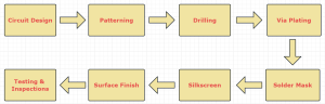
The PCB Manufacturing Process varies according to PCB structure and technology, but a typical rigid multilayer PCB may involve the following major stages.
1. PCB Design and Manufacturing Data
PCB production begins with a completed design.
The engineering team prepares manufacturing data such as:
- Gerber or other fabrication data
- Drill files
- Stackup information
- Board outline
- Copper weights
- Surface finish requirements
- Solder mask information
- Silkscreen data
- Special process requirements
The manufacturer reviews these files to identify potential manufacturing issues.
2. Engineering Review and DFM
Before production, the manufacturer performs a DFM review.
DFM evaluation may check:
- Minimum trace width
- Minimum spacing
- Pad dimensions
- Hole sizes
- Annular rings
- Copper-to-edge clearance
- Solder mask clearance
- Layer registration
- Impedance requirements
- Surface finish compatibility
- Manufacturing tolerances
A design that is electrically correct may still require modification if it cannot be produced reliably with the selected manufacturing process.
3. Material Preparation
The appropriate laminate, copper foil, prepreg, and other materials are prepared according to the approved stackup.
Material selection should consider electrical performance, thermal requirements, mechanical properties, reliability, and application environment.
4. Inner-Layer Imaging
For multilayer boards, the required circuit pattern is transferred onto the copper surface of the inner-layer cores.
A photosensitive material is exposed using imaging equipment, and the unwanted copper is subsequently removed during etching.
5. Etching and Stripping
The exposed copper pattern is chemically etched to remove unwanted copper.
The remaining copper forms the required circuit traces and pads.
After etching, the imaging material is stripped away and the circuit is cleaned and inspected.
6. Layer Inspection
Inner-layer circuits are inspected before lamination.
Automated optical inspection can identify issues such as:
- Open circuits
- Shorts
- Incorrect features
- Missing copper
- Over-etching
- Under-etching
Early inspection is important because defects trapped inside a multilayer stack become significantly more difficult to correct after lamination.
7. Lamination
The inner-layer cores and prepreg materials are stacked according to the approved layer configuration.
Heat and pressure are applied according to the selected material system and lamination process. The resin in the prepreg flows and cures, creating a consolidated multilayer PCB.
Layer alignment and registration are critical during this stage.
8. Drilling
Mechanical drilling is commonly used for conventional through-holes, while laser drilling can be used for microvias and certain advanced structures.
Drilling quality can be affected by:
- Tool wear
- Drill parameters
- Material structure
- Hole diameter
- Board thickness
- Stackup configuration
Important quality indicators include hole diameter, position accuracy, wall condition, burrs, and hole cleanliness.
9. Desmear and Hole Preparation
After drilling, resin smear may remain on the hole walls.
A desmear process can remove unwanted resin and prepare the hole walls for reliable metallization.
The exact chemical process depends on the material system and board construction.
10. Electroless Copper and Electroplating
Copper plating creates a conductive layer on the prepared hole walls and PCB surfaces.
An electroless copper process can establish an initial conductive layer, followed by electrolytic copper plating to build the required copper thickness.
Plating quality is critical for via reliability and current-carrying performance.
11. Outer-Layer Circuit Formation
The outer copper layers are patterned using imaging and etching processes.
Depending on the manufacturing method, copper may be plated to build the required thickness before the final etching operation.
Process control is essential to maintain trace width, spacing, registration, and copper thickness.
12. Solder Mask Application
The solder mask is applied to protect the PCB surface and expose only the required pads and contact areas.
After imaging and curing, the board is inspected for issues such as:
- Mask misregistration
- Insufficient coverage
- Pinholes
- Peeling
- Contamination
- Incomplete curing
13. Surface Finish
An appropriate surface finish is applied to exposed copper pads and other specified areas.
The selected finish should match the assembly process, component requirements, shelf-life expectations, and intended application.
14. Silkscreen and Marking
Silkscreen or other marking processes add reference designators, polarity indicators, logos, part numbers, date codes, and other required information.
Marking must remain legible without interfering with solder pads or electrical contacts.
15. Profiling and Routing
The finished PCB panel is separated into individual boards using routing, milling, punching, V-scoring, or a combination of methods depending on board design.
Dimensional accuracy is particularly important for boards that must fit into precise mechanical assemblies.
16. Electrical Testing and Final Inspection
Finished boards undergo appropriate electrical and visual inspections before shipment.
Testing may include:
- Flying probe testing
- Fixture-based electrical testing
- Continuity testing
- Isolation testing
- Visual inspection
- Automated optical inspection
- Dimensional inspection
The appropriate test method depends on production volume, board complexity, test-point accessibility, and customer requirements.
Multilayer PCB Manufacturing
The production of a Multilayer PCB requires additional processes compared with single- or double-sided boards.
Individual inner-layer cores are first fabricated and inspected. These cores are then stacked with prepreg according to the specified layer sequence.
During lamination, heat and pressure bond the stack into a single multilayer structure.
After lamination, the board undergoes drilling, hole preparation, copper plating, outer-layer pattern formation, solder mask, surface finishing, marking, profiling, and final testing.
Important multilayer manufacturing factors include:
- Layer registration
- Lamination thickness
- Resin flow
- Dielectric thickness
- Copper distribution
- Thermal expansion
- Via reliability
- Controlled impedance
For high-speed designs, the PCB stackup must be considered together with trace geometry, dielectric properties, reference planes, and manufacturing tolerances.
PCB Testing and Inspection
Testing is an essential part of PCB Testing and quality control. Different inspection methods identify different categories of defects, so no single inspection method can detect every possible manufacturing problem.
Visual Inspection
Visual inspection can identify obvious defects such as:
- Scratches
- Contamination
- Solder mask damage
- Silkscreen problems
- Surface-finish abnormalities
- Mechanical damage
Automated Optical Inspection
AOI uses cameras and image-processing algorithms to inspect PCB features against defined criteria or reference data.
AOI can identify many visible manufacturing defects, including:
- Missing or incorrect features
- Shorts
- Open patterns
- Trace defects
- Registration errors
- Solder mask-related issues
AOI is an inspection technology rather than a complete electrical or functional test.
Electrical Testing
Electrical testing verifies electrical continuity and isolation according to the test strategy.
Common approaches include flying probe testing and fixture-based testing.
Flying Probe Testing
Flying probe testing uses programmable probes to contact selected test points on the PCB.
It is particularly useful for prototypes and low-volume production because it can reduce the need for dedicated test fixtures.
Its relatively flexible setup makes it suitable for frequent design changes.
Fixture-Based Electrical Testing
Fixture-based testing uses dedicated test fixtures to contact multiple points on a PCB.
It can provide high throughput for stable, higher-volume production but usually requires additional fixture development and cost.
X-Ray Inspection
X-ray inspection can be used when internal structures or hidden features need to be examined.
For PCB manufacturing and assembly applications, X-ray can help inspect:
- Via structures
- Internal connections
- Plated holes
- Hidden solder joints after assembly
X-ray should be selected according to the actual inspection requirement rather than being treated as a mandatory test for every PCB.
Common PCB Manufacturing Defects
Typical manufacturing problems include:
| Defect | Possible Causes |
|---|---|
| Open circuit | Over-etching, missing copper, process damage |
| Short circuit | Insufficient spacing, under-etching, contamination |
| Hole size variation | Drill wear, incorrect parameters |
| Poor plating | Surface preparation or plating-process issues |
| Solder mask misalignment | Registration or imaging problems |
| Delamination | Material incompatibility, lamination process issues |
| Warpage | Material structure, copper imbalance, thermal history |
| Surface-finish defects | Process contamination or chemistry control |
| Dimensional variation | Profiling, lamination, or material-related factors |
Root-cause analysis should consider the complete manufacturing process rather than focusing only on the final inspection result.
Current and Future Trends in PCB Manufacturing
The electronics industry continues to push PCB technology toward higher density, greater functionality, improved electrical performance, and smaller form factors.
Miniaturization
Smaller electronic products require increasingly dense PCB structures.
This drives the development of:
- Fine-line circuitry
- Microvias
- HDI technology
- Advanced substrate materials
- Embedded components
- High-density packaging
High-Speed and High-Frequency Electronics
High-speed processors, data centers, networking equipment, radar, wireless communication, and other advanced systems require PCBs with carefully controlled electrical characteristics.
Material selection, stackup design, impedance control, trace geometry, return paths, and manufacturing tolerances all become increasingly important.
Automotive Electronics and EVs
Advanced driver assistance systems, electric vehicles, battery systems, charging infrastructure, and vehicle networking are increasing the demand for high-reliability PCBs.
Automotive applications also place greater emphasis on thermal management, vibration resistance, environmental reliability, and electromagnetic compatibility.
IoT and Smart Devices
IoT products combine sensors, processors, wireless connectivity, and power management in compact form factors.
This trend continues to encourage the use of flexible circuits, HDI structures, miniaturized components, and highly integrated PCB designs.
Sustainable PCB Manufacturing
Environmental considerations are becoming increasingly important throughout PCB production.
Manufacturers are working to improve:
- Material efficiency
- Chemical management
- Energy consumption
- Waste reduction
- Recycling
- Process efficiency
Sustainable manufacturing must also consider product reliability and regulatory requirements rather than focusing only on material reduction.
How to Improve PCB Manufacturing Quality
High-quality PCB production depends on controlling the entire manufacturing chain.
Important practices include:
- Conduct a thorough engineering review before production.
- Use a clearly defined PCB stackup.
- Select materials according to actual electrical, thermal, and mechanical requirements.
- Perform DFM analysis before fabrication.
- Maintain controlled manufacturing parameters.
- Monitor drilling and plating processes carefully.
- Control multilayer registration during lamination.
- Inspect inner layers before they are laminated.
- Select the surface finish according to the assembly application.
- Use appropriate electrical and visual inspection methods.
- Maintain complete production and test records.
- Apply strict revision control to manufacturing data.
Early collaboration between PCB designers and manufacturers can significantly reduce avoidable manufacturing problems.
Kingda PCB Manufacturing Support
Kingda provides PCB manufacturing support for projects requiring different board structures, materials, layer configurations, and manufacturing technologies.
Depending on project requirements, the manufacturing workflow can include:
- Engineering and manufacturability review
- Material selection support
- PCB fabrication
- Multilayer PCB manufacturing
- HDI and high-density structures
- Flexible and rigid-flex PCB manufacturing
- Surface finishing
- Electrical testing
- Visual and automated inspection
- Manufacturing documentation
- Production support
Kingda can also coordinate PCB fabrication requirements with PCB assembly considerations, helping ensure that the bare board is suitable for the intended downstream assembly and testing process.
How to Select a PCB Manufacturing Partner
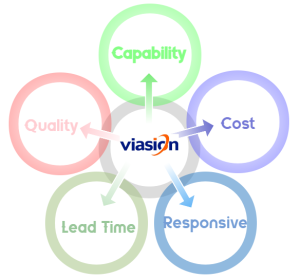
When selecting a PCB manufacturer, consider more than the quoted unit price.
Important evaluation factors include:
- Manufacturing technology
- Material capabilities
- Layer-count capability
- Minimum feature sizes
- Copper thickness capability
- Via technology
- Controlled impedance capability
- Surface-finishing options
- Inspection and testing resources
- Engineering support
- DFM review capability
- Production capacity
- Quality management
- Traceability
- Communication and engineering change control
The manufacturer should be able to clearly explain which technologies are standard, which require special processing, and which specifications may affect cost or production time.
Conclusion
PCB Manufacturing is a complex engineering and production process that transforms a circuit design into a reliable physical board. The process includes material preparation, circuit imaging, etching, lamination, drilling, plating, solder mask application, surface finishing, marking, profiling, inspection, and PCB Testing.
Different applications require different PCB structures. Single-sided and double-sided boards are suitable for relatively simple designs, while Multilayer PCB, flexible, rigid-flex, and HDI PCB technologies enable higher density and more advanced electronic systems.
As electronic products become smaller, faster, and more connected, PCB manufacturing will continue to evolve toward higher density, improved signal integrity, advanced materials, better thermal performance, automotive-grade reliability, and more sustainable production.
A successful PCB project therefore requires close coordination among PCB design, material selection, DFM, fabrication, testing, assembly, and quality control. Selecting a capable manufacturing partner at an early stage can help reduce manufacturing risks and create a smoother transition from PCB design to stable production.