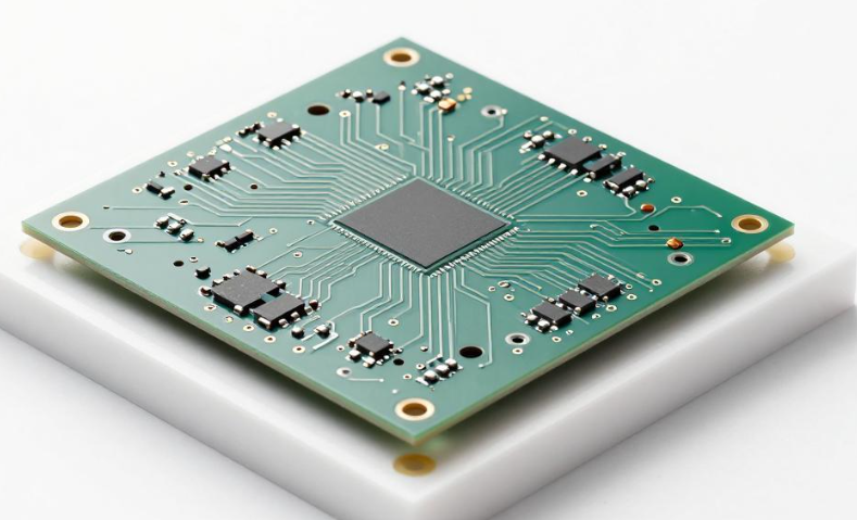
Switching from conventional PCB materials to Halogen-Free PCB materials is not simply a matter of changing the laminate specification in the BOM. Halogen-free laminates can have different resin systems, glass-fiber characteristics, thermal behavior, drilling performance, and lamination requirements compared with conventional FR-4 materials.
A PCB design that performs normally during prototype production may encounter manufacturing and reliability problems during volume production if the design does not account for these material differences. Potential issues can include rough hole walls, poor plating adhesion, delamination, solder mask adhesion problems, board cracking, and dimensional instability.
Therefore, Halogen-Free PCB Design should consider material characteristics from the beginning of the engineering process. Stackup construction, prepreg selection, hole dimensions, annular rings, copper distribution, panelization, solder mask design, impedance control, and manufacturing tolerances should all be reviewed through a DFM perspective.
The goal is not to create an entirely different design methodology, but to adapt the existing PCB Design to the actual processing characteristics of halogen-free materials so that prototype performance can be transferred more reliably to volume production.
Why Halogen-Free PCB Design Requires Special Attention
Halogen-free PCB materials are designed to meet defined halogen-content requirements while maintaining the electrical, thermal, and mechanical properties required by the application.
However, different halogen-free laminate systems can have significantly different material properties. Depending on the material family, engineers may encounter differences in:
- Resin chemistry
- Glass-transition temperature (Tg)
- Decomposition temperature (Td)
- Coefficient of thermal expansion (CTE)
- Dielectric constant (Dk)
- Dissipation factor (Df)
- Resin flow behavior
- Moisture absorption
- Drilling characteristics
- Thermal expansion in the Z-axis
- Lamination process window
These properties directly influence the manufacturing process.
For this reason, designers should avoid treating all halogen-free laminates as interchangeable. The selected material should be evaluated together with the manufacturer’s fabrication process and the requirements of the final application.
1. PCB Stackup and Prepreg Selection
Match the Stackup to the Halogen-Free Resin System
The PCB Stackup is one of the most important considerations when converting an existing PCB design to a halogen-free material system.
A multilayer PCB is typically constructed from copper-clad cores and prepreg. During lamination, heat and pressure cause the resin in the prepreg to soften, flow, and cure, bonding the individual layers together.
Because different resin systems can have different curing behavior and resin-flow characteristics, an existing prepreg combination should not automatically be reused when changing materials.
An appropriate stackup review should consider:
- Core thickness
- Copper thickness
- Prepreg type
- Resin content
- Final dielectric thickness
- Resin flow
- Lamination pressure
- Lamination temperature
- Cure profile
- Layer registration
- Finished board thickness
The correct combination of core and prepreg should be confirmed with the laminate supplier and PCB manufacturer.
Control Dk and Df for High-Speed Designs
For high-speed applications, material selection affects signal integrity and Impedance Control.
Engineers should obtain reliable Dk and Df data for the selected halogen-free laminate rather than simply transferring simulation parameters from a conventional FR-4 material.
For demanding high-speed designs, it may be necessary to evaluate:
- Dk at the relevant frequency
- Df at the relevant frequency
- Test-method differences
- Temperature dependence
- Resin-content effects
- Effective dielectric constant
- Finished dielectric thickness
Material data should be used consistently in stackup calculations and simulation.
If the dielectric properties change significantly between the prototype material and production material, the actual impedance may deviate from the original design target.
Clearly Specify the Complete Material System
A common mistake is to specify only a halogen-free core material while leaving the prepreg specification unclear.
For a multilayer board, the entire material system should be defined, including:
- Core material
- Prepreg family
- Copper foil
- Solder mask
- Surface finish
- Required halogen limits
- Applicable material specifications
The core and prepreg should be compatible with each other and with the intended lamination process.
This is particularly important when the product has strict environmental or regulatory requirements. Simply using a halogen-free core does not automatically make the entire PCB halogen-free.
2. Hole Diameter and Annular Ring Design
Consider Drilling Characteristics
Drilling is an important manufacturing step for both through-holes and advanced via structures.
The drilling behavior of a laminate can vary according to its resin system, glass-fiber structure, board thickness, copper thickness, drill diameter, and process conditions.
Potential manufacturing problems include:
- Rough hole walls
- Resin smear
- Glass-fiber protrusion
- Burrs
- Hole-position deviation
- Hole-size variation
- Reduced plating adhesion
Drill-tool wear is also affected by board construction and production conditions. Therefore, designers should avoid selecting extremely small holes or excessively high aspect ratios unless the manufacturer’s process capability has been verified.
Avoid Extreme Aspect Ratios
The aspect ratio of a plated through-hole is generally calculated as:
Aspect Ratio = PCB Thickness ÷ Finished Hole Diameter
As the aspect ratio increases, hole-wall preparation and copper plating become more demanding.
For halogen-free multilayer boards with high aspect ratios, the manufacturer should confirm:
- Mechanical drilling capability
- Desmear capability
- Hole-wall quality
- Electroless copper coverage
- Electroplating capability
- Finished-hole tolerance
- Reliability requirements
Designers should not rely on a universal maximum aspect ratio because the practical limit depends on the PCB manufacturer, material system, board thickness, and hole technology.
Annular Ring Design
The annular ring provides copper around a drilled hole and contributes to reliable electrical and mechanical connection.
When designing annular rings, consider:
- Drill tolerance
- Registration tolerance
- Etching tolerance
- Plating requirements
- Finished-hole size
- Pad size
- Manufacturing capability
Avoid designing annular rings at the absolute minimum process limit unless there is a strong technical reason to do so.
A reasonable manufacturing margin can help reduce the risk of breakout and unreliable via connections during volume production.
3. Copper Thickness, Layout, and Panelization
Copper Distribution
Copper thickness and copper distribution can influence both electrical performance and manufacturing reliability.
Heavy-copper designs can introduce additional thermal and mechanical stress during lamination and thermal processing. This becomes more important when thick copper is combined with multilayer structures or large differences in copper density between layers.
Designers should therefore review:
- Copper weight
- Current-carrying requirements
- Copper density by layer
- Large copper areas
- Thermal expansion
- Plating requirements
- Finished board thickness
Balance Copper Across the PCB
Large differences in copper distribution can contribute to uneven etching, lamination behavior, and board warpage.
Where electrically appropriate, designers can use copper balancing techniques to create a more uniform distribution of copper across the panel.
However, copper balancing should not compromise:
- Signal integrity
- Power integrity
- Controlled impedance
- Thermal requirements
- Creepage and clearance
- High-voltage isolation
Panelization and V-Cut Design
Panelization is often overlooked during PCB design, but it can have a significant impact on volume manufacturing.
For halogen-free boards, the designer and manufacturer should consider:
- Board thickness
- Material mechanical strength
- V-Cut depth
- Routing depth
- Breakaway tabs
- Tab-hole structures
- Panel size
- Board spacing
- Component clearance
- Depanelization stress
Excessive V-Cut depth can weaken the remaining material and increase mechanical stress during depanelization.
For larger or mechanically sensitive boards, routed breakaway structures may be more appropriate than relying entirely on V-Cut.
The final panel design should be reviewed with the PCB manufacturer before production release.
4. Heavy-Copper Halogen-Free PCBs
Heavy-copper Halogen-Free PCB designs require additional attention because thick copper can increase thermal mass and affect the overall thermal-mechanical behavior of the PCB.
Potential considerations include:
- Copper-to-dielectric stress
- Z-axis expansion
- Lamination compatibility
- Plating thickness
- Thermal cycling
- Via reliability
- Copper distribution
- Board warpage
Large copper areas may also affect resin flow during lamination. The stackup and copper distribution should therefore be reviewed together.
For high-current applications, thermal vias, copper planes, thicker copper, and appropriate heat-dissipation structures may be required.
High-Voltage Design
Halogen-free materials may offer useful electrical and thermal characteristics for certain applications, but designers should not automatically reduce creepage or clearance distances simply because a particular material has favorable CTI characteristics.
High-voltage designs must continue to comply with the applicable safety standards and product-specific requirements.
Important factors include:
- Working voltage
- Pollution degree
- Material group
- Altitude
- Creepage distance
- Clearance
- Insulation system
- Applicable safety standard
Material properties can support the design, but they do not replace the requirements of the applicable safety standard.
5. Solder Mask and Surface Finish
Specify the Solder Mask System
The solder mask is part of the overall material system and should be specified appropriately when manufacturing a Halogen-Free PCB.
If the product has a halogen-free material requirement, the designer should clearly communicate whether the solder mask and other non-laminate materials must also comply with the customer’s specified halogen limits.
The PCB manufacturer should verify compatibility between the solder mask system and the selected laminate.
Solder Mask Design
Solder mask design should avoid unnecessary process extremes.
Important considerations include:
- Solder mask clearance
- Minimum solder mask bridge
- Pad-to-mask spacing
- Large copper-area openings
- Fine-pitch components
- Via-in-pad structures
- Surface-finish compatibility
Extremely narrow solder mask bridges or unusually large openings may increase manufacturing sensitivity.
Surface Finish
Common surface finishes such as:
- HASL
- Lead-free HASL
- ENIG
- ENEPIG
- OSP
- Immersion silver
- Immersion tin
can be used with different PCB material systems when properly specified and processed.
The appropriate surface finish depends on:
- Assembly process
- Solderability requirements
- Shelf life
- Contact requirements
- Environmental conditions
- Fine-pitch component requirements
- Cost considerations
For high-temperature processing, moisture management and material compatibility should be evaluated according to the laminate and assembly supplier’s recommendations.
6. Moisture Management
Moisture can affect PCB processing and reliability, particularly during high-temperature manufacturing processes.
A moisture-sensitive board may experience:
- Delamination
- Blistering
- Dimensional changes
- Reduced interlayer adhesion
- Reliability degradation
However, there is no single universal baking temperature or baking time that applies to every halogen-free PCB.
Baking requirements should be determined according to:
- Laminate manufacturer’s recommendations
- Storage conditions
- Exposure time
- Board thickness
- Surface finish
- Assembly process
- Moisture sensitivity requirements
Proper packaging and storage can reduce unnecessary moisture exposure before assembly.
7. Design for Manufacturing and Reliability
A successful Halogen-Free PCB Design should consider manufacturing constraints before the first prototype is released.
A comprehensive DFM review can evaluate:
Electrical Design
- Trace width and spacing
- Controlled impedance
- Differential pairs
- Return paths
- Power distribution
- High-voltage isolation
Mechanical Design
- Board thickness
- Board dimensions
- Mounting holes
- Edge clearance
- Panelization
- Depanelization method
- Connector locations
Fabrication Design
- Minimum hole size
- Aspect ratio
- Annular ring
- Copper thickness
- Layer registration
- Solder mask clearance
- Surface finish
Material Design
- Core material
- Prepreg
- Copper foil
- Dk/Df
- Tg/Td
- CTE
- Halogen requirements
- Thermal performance
Reliability Design
- Thermal cycling
- Mechanical stress
- Vibration
- Humidity
- High-temperature exposure
- Via reliability
- Interlayer adhesion
8. Halogen-Free PCB Design for High-Speed Applications
High-speed boards require more than simply selecting a halogen-free laminate.
The material, stackup, trace geometry, and reference planes must work together.
Important factors include:
- Dk and Df
- Dielectric thickness
- Trace width
- Trace spacing
- Copper roughness
- Reference-plane continuity
- Via transitions
- Differential-pair geometry
- Return-current paths
- Impedance tolerance
For high-speed applications, engineers should use supplier-specific material data and verify the finished stackup with the PCB manufacturer.
If the PCB uses a different material during mass production than during prototyping, impedance and insertion-loss performance may change.
Therefore, prototype and production materials should be controlled through the approved material specification.
9. Halogen-Free PCB Design Checklist
Before releasing a Halogen-Free PCB design for volume production, engineers can use the following checklist:
- Confirm that all specified cores and prepregs meet the required halogen limits.
- Clearly define the complete PCB material system.
- Verify Tg, Td, Dk, Df, CTE, and other relevant material properties.
- Confirm that the stackup is compatible with the selected laminate system.
- Check hole diameter and aspect ratio against the manufacturer’s process capability.
- Provide sufficient annular-ring margin.
- Review heavy-copper structures and copper distribution.
- Verify panelization and depanelization requirements.
- Review V-Cut and routing structures for mechanical stress.
- Confirm solder mask material and design requirements.
- Select a compatible surface finish.
- Define moisture-storage and pre-processing requirements where applicable.
- Use appropriate temperature-dependent material data for high-speed simulations.
- Verify controlled-impedance requirements against the actual production stackup.
- Complete a DFM review before mass production.
- Confirm that all manufacturing documents use the same approved material and process specifications.
10. Common Design Mistakes When Switching to Halogen-Free Materials
Several mistakes frequently occur when an existing PCB design is converted to a new material system.
Mistake 1: Changing Only the Core Material
Replacing the conventional core with a halogen-free core while leaving the prepreg and other material specifications unchanged can create material-system incompatibility.
Better approach: define and approve the complete stackup.
Mistake 2: Copying the Original Stackup
The original stackup may have been optimized for another laminate’s Dk, Df, resin content, and lamination characteristics.
Better approach: recalculate the stackup using the selected material supplier’s data.
Mistake 3: Using the Same Extreme Hole Dimensions
A hole specification that is easy to manufacture with one material system may be more challenging with another.
Better approach: compare the design against actual drilling and plating capabilities.
Mistake 4: Ignoring Copper Distribution
Large differences in copper density can influence lamination and warpage.
Better approach: review copper distribution across all layers.
Mistake 5: Treating Halogen-Free as a Single Material Category
Not every halogen-free laminate has identical electrical, thermal, mechanical, or processing properties.
Better approach: evaluate the specific laminate family and manufacturer data.
Mistake 6: Treating Prototype Results as Proof of Mass-Production Capability
A prototype may use different equipment settings, smaller quantities, different panelization, or more intensive manual inspection.
Better approach: conduct a production-oriented DFM review before volume manufacturing.
11. How Kingda Supports Halogen-Free PCB Projects
Kingda can support Halogen-Free PCB projects by incorporating material requirements and manufacturing considerations into the PCB fabrication workflow.
Depending on project requirements, engineering support may include:
- Material and stackup review
- Prepreg selection support
- Hole and via design review
- Copper-thickness evaluation
- Impedance-control review
- Panelization review
- Solder mask and surface-finish evaluation
- DFM analysis
- Manufacturing documentation review
- PCB fabrication
- Electrical testing and inspection
For high-speed, high-density, heavy-copper, or other demanding PCB designs, early communication between the designer and manufacturer can help identify process limitations before production.
The specific material system, tolerances, and manufacturing capability should always be confirmed against the approved project specifications.
Conclusion
A Halogen-Free PCB should not be treated as a conventional PCB with a different laminate name. Changes in resin chemistry, glass-fiber structure, dielectric properties, thermal behavior, drilling characteristics, and lamination performance can affect the entire manufacturing process.
A successful Halogen-Free PCB Design therefore requires coordinated consideration of the PCB Stackup, PCB Materials, hole and annular-ring dimensions, copper distribution, panelization, solder mask, surface finish, moisture management, and DFM requirements.
For high-speed applications, Impedance Control should be based on accurate material data and the actual production stackup rather than copied from an existing conventional FR-4 design.
Most importantly, the goal of design optimization is not simply to make a prototype work. The design should be robust enough to maintain electrical performance, manufacturability, and reliability when transferred to volume production.
By evaluating material characteristics early and communicating manufacturing requirements clearly, engineers can reduce production risks and build a more reliable path from prototype validation to stable PCB Manufacturing.