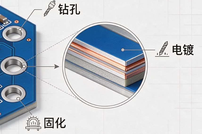
In high-volume PCB production, unnecessarily customized via dimensions can become an overlooked source of manufacturing complexity. Engineers sometimes select different hole diameters and pad sizes to accommodate local routing requirements without considering the downstream impact on drilling, plating, inspection, and production scheduling.
Although a small dimensional change may appear insignificant at the design stage, introducing too many PCB via hole sizes can increase the number of drilling tools required, complicate process setup, and reduce manufacturing efficiency. When several non-standard dimensions are mixed on the same board, the PCB manufacturer may also need additional tooling and process verification.
A better approach is to establish a practical via standardization strategy during PCB layout. By using a controlled set of commonly supported via hole size and pad dimensions, designers can simplify manufacturing while maintaining the electrical, mechanical, and reliability requirements of the PCB.
For projects manufactured by Kingda, via dimensions can be reviewed together with board thickness, copper thickness, aspect ratio, component pitch, routing density, and fabrication capabilities to determine an appropriate standardization strategy.
1. Hidden Costs and Manufacturing Risks of Excessive Via Sizes
The cost and manufacturability of PCB drilling are closely related to tooling, drilling parameters, board construction, production volume, and process control.
When a PCB design contains many different hole diameters, the manufacturer may need to manage more drill tools and additional tool changes. This can increase setup requirements and complicate production planning.
A standardized PCB drilling strategy, by comparison, allows manufacturers to consolidate similar operations and establish repeatable process parameters. This can improve production consistency and reduce unnecessary tooling complexity.
Tooling and Setup Complexity
Mechanical drills are selected according to the required finished hole size and manufacturing process. Using uncommon or project-specific dimensions may require dedicated tooling or additional tool management.
For high-volume production, even small increases in setup and tooling requirements can accumulate into meaningful manufacturing costs.
However, the definition of a “standard” hole size varies between PCB manufacturers. Designers should therefore avoid assuming that a particular diameter is universally standard. Instead, the preferred approach is to obtain the manufacturer’s design rules and capability table before finalizing the PCB layout.
Drilling Quality
Very small mechanical holes can increase manufacturing difficulty, particularly when the board has a high layer count, large thickness, high copper thickness, or demanding aspect ratio.
Potential issues can include drill wander, hole-position deviation, burrs, resin smear, or damage to the surrounding laminate. These risks depend on the complete PCB construction rather than hole diameter alone.
For this reason, via hole size should be selected according to both electrical requirements and manufacturing capability.
Pad and Annular Ring Considerations
Reducing the hole diameter without appropriately adjusting the via pad can create insufficient annular ring.
The annular ring is important for maintaining reliable electrical connection between the drilled hole and the surrounding copper pad. Its required size should be calculated based on the PCB manufacturer’s registration capability, finished hole tolerance, copper structure, and applicable design rules.
Rather than applying one fixed minimum value to every PCB, designers should use the fabrication supplier’s capability specifications.
2. Establishing a Practical Via Standardization Strategy
A useful via standardization strategy does not mean forcing every PCB to use one single hole diameter. Instead, it means limiting the design to a small number of well-defined via families whenever the electrical and mechanical requirements allow it.
For example, a design team may establish preferred dimensions for:
- General signal vias
- Ground and power vias
- Thermal or current-carrying vias
- BGA fan-out vias
- Blind or buried vias where required
- Special high-density interconnect structures
The actual dimensions should be selected according to the PCB manufacturer’s capabilities and the requirements of the application.
General Signal Vias
For conventional through-hole vias, designers often use relatively moderate drill diameters and pad sizes because they provide a practical balance between routing density, manufacturability, and reliability.
A commonly used design such as a 0.30 mm finished hole with an appropriately sized pad may work well for many conventional applications, but it should not be treated as a universal requirement.
The appropriate PCB via hole should be determined after considering:
- Board thickness
- Finished hole tolerance
- Layer count
- Routing density
- Required annular ring
- Signal integrity requirements
- PCB manufacturer capabilities
Power and Ground Vias
Power and ground connections may require larger or multiple vias depending on current, temperature rise, copper thickness, and thermal requirements.
Instead of simply increasing the diameter of one via, designers can often use multiple vias in parallel to distribute current and improve thermal transfer.
For high-current applications, via selection should therefore be based on the complete current path rather than a simple “larger hole equals higher current” rule.
The design should consider via barrel copper thickness, number of vias, pad geometry, surrounding copper area, thermal conditions, and allowable temperature rise.
High-Density and BGA Applications
High-density packages such as BGAs may require smaller vias to provide sufficient routing space.
However, simply reducing the via diameter is not always the best solution. Designers can also improve routing density through optimized fan-out patterns, via placement, trace width, layer allocation, and escape routing.
Where the package pitch and fabrication capability allow it, standard or established small-via dimensions should be preferred over unusual custom dimensions.
For particularly dense BGA layouts, technologies such as microvias, via-in-pad, and HDI structures may be necessary. These processes should be evaluated with the PCB manufacturer before design completion because they involve different manufacturing requirements from conventional through-hole vias.
3. Coordinate Via Size With PCB Manufacturing Processes
Standardizing hole dimensions becomes more valuable when the design is coordinated with downstream manufacturing processes.
Simplify Drilling
A controlled number of PCB drilling diameters can reduce tool changes and make production programming easier.
It can also help manufacturers establish stable drilling parameters and simplify tool-life management. However, the exact improvement depends on the number of boards, panel utilization, drilling equipment, and existing factory process flow.
The objective is not simply to minimize the number of drill sizes. It is to eliminate unnecessary variations while retaining dimensions that provide genuine design value.
Improve Plating Consistency
After drilling, through-holes generally require desmear and metallization/plating processes to establish electrical connections between layers.
Hole size, board thickness, aspect ratio, copper thickness, and plating chemistry can all influence the achievable plating quality.
Standardized via dimensions can make process control more predictable, but they do not automatically guarantee uniform plating. Proper chemical control, current distribution, agitation, pretreatment, and inspection remain essential.
Standardize Solder Mask Treatment
Via solder mask treatment should also be considered during PCB design.
Depending on the application, vias may be:
- Tented with solder mask
- Opened on one or both sides
- Plugged or filled
- Used as via-in-pad structures
The correct option depends on soldering requirements, contamination protection, thermal considerations, test access, and component packaging.
Standardizing the treatment of conventional vias can reduce unnecessary process variation, but special vias may still require customized processing.
4. Avoid Over-Standardization
While standardization provides significant manufacturing advantages, excessive standardization can also create design problems.
A single via dimension should not be forced into every application if it causes:
- Insufficient routing space
- Excessive parasitic capacitance
- Poor current capacity
- Inadequate thermal performance
- Insufficient annular ring
- BGA escape-routing limitations
- Excessive impedance discontinuity
- Violation of PCB fabrication rules
For high-speed designs, via geometry can affect signal integrity because a via introduces discontinuity in the transmission path. Designers may need to evaluate via stub length, antipad dimensions, reference-plane transitions, differential-pair symmetry, and return-current paths.
Therefore, the engineering objective should be controlled standardization, not blind standardization.
5. Practical Rules for Selecting Standard Via Dimensions
Before releasing PCB fabrication data, engineers can use the following checklist:
1. Check the PCB manufacturer’s capability first.
Confirm the standard mechanical drill sizes, minimum finished hole, hole tolerance, annular ring capability, and recommended pad dimensions.
2. Minimize unnecessary drill variations.
If two different via sizes provide essentially the same electrical and mechanical function, consider consolidating them into one preferred dimension.
3. Match the via to the board thickness.
The hole diameter should be evaluated together with the finished board thickness and aspect ratio.
4. Verify the annular ring.
Do not select a pad size based only on nominal dimensions. Account for drill tolerance, registration, and manufacturing capability.
5. Separate signal and power requirements.
Signal vias, power vias, thermal vias, and high-current structures may require different geometries.
6. Evaluate high-speed effects.
For high-speed interfaces, consider the electrical effect of the complete via structure rather than selecting dimensions only from a mechanical perspective.
7. Review special structures with the manufacturer.
Microvias, blind vias, buried vias, via-in-pad, and filled vias should be reviewed during the DFM stage.
6. The Manufacturing Value of Via Standardization
A well-designed via standardization strategy can provide several benefits throughout the PCB manufacturing process.
First, it can reduce tooling diversity and simplify drilling programs. Second, it can make process setup and inspection more consistent. Third, it can simplify production documentation and DFM review. Finally, it can make future revisions easier because designers can reuse established via structures.
For repeated products, these benefits become particularly valuable. Once a preferred via library has been validated for a specific PCB manufacturing process, the same structures can be reused across product revisions or related board designs.
This creates a more consistent design-to-manufacturing workflow and reduces the need to repeatedly introduce new fabrication parameters.
However, the actual cost reduction cannot be represented by one universal percentage. Savings depend on PCB dimensions, order quantity, layer count, hole count, tooling strategy, panelization, and factory utilization.
The most reliable method is to compare the manufacturer’s quotation and process requirements before and after design standardization.
7. Kingda’s Approach to Standardized PCB Via Design
At Kingda, via design can be evaluated from both the electrical and manufacturing perspectives.
Instead of recommending a single fixed hole diameter for every PCB, Kingda can review the complete design requirements, including:
- Board thickness and layer count
- Finished hole dimensions
- Copper thickness
- Via and pad geometry
- Annular ring requirements
- Current-carrying requirements
- BGA and high-density routing
- High-speed signal integrity
- HDI requirements
- Surface and solder mask treatment
- Production volume
This approach helps engineers identify which via dimensions can be standardized and which ones genuinely require specialized processing.
For high-volume products, reducing unnecessary via variations can make PCB production more repeatable and easier to manage. For prototypes and complex boards, maintaining the necessary specialized structures may be more appropriate.
The goal is to achieve the best balance between design flexibility, manufacturing capability, cost, and long-term reliability.
8. Conclusion
PCB via hole selection is not simply a layout decision. It directly influences drilling, plating, pad design, routing density, inspection, and manufacturing efficiency.
Using a controlled range of standard via hole size and via pad dimensions can reduce unnecessary tooling complexity and simplify PCB production, especially for products manufactured in repeated or high-volume quantities.
At the same time, engineers should avoid treating standardization as a rigid rule. High-current circuits, high-speed interfaces, BGA packages, HDI structures, and other specialized applications may require different via geometries.
The most effective strategy is to establish a standardized via library based on actual PCB fabrication capabilities, then allow carefully justified exceptions when electrical or mechanical requirements demand them.
By combining DFM principles with controlled PCB drilling and via standardization, engineers can simplify manufacturing, improve process consistency, and control PCB manufacturing cost while preserving the performance and reliability required by the final product.