In high-density PCB manufacturing, small geometric errors in Gerber data can become significant production problems. This is especially important for fine-pitch packages such as QFN, BGA, and other components with tight pad-to-pad spacing.
A Gerber file may pass standard CAM inspection while the finished PCB still shows unexpected pad displacement. When the error is systematic rather than random, engineers should investigate not only the original design data but also how the manufacturing system interprets and converts that geometry.
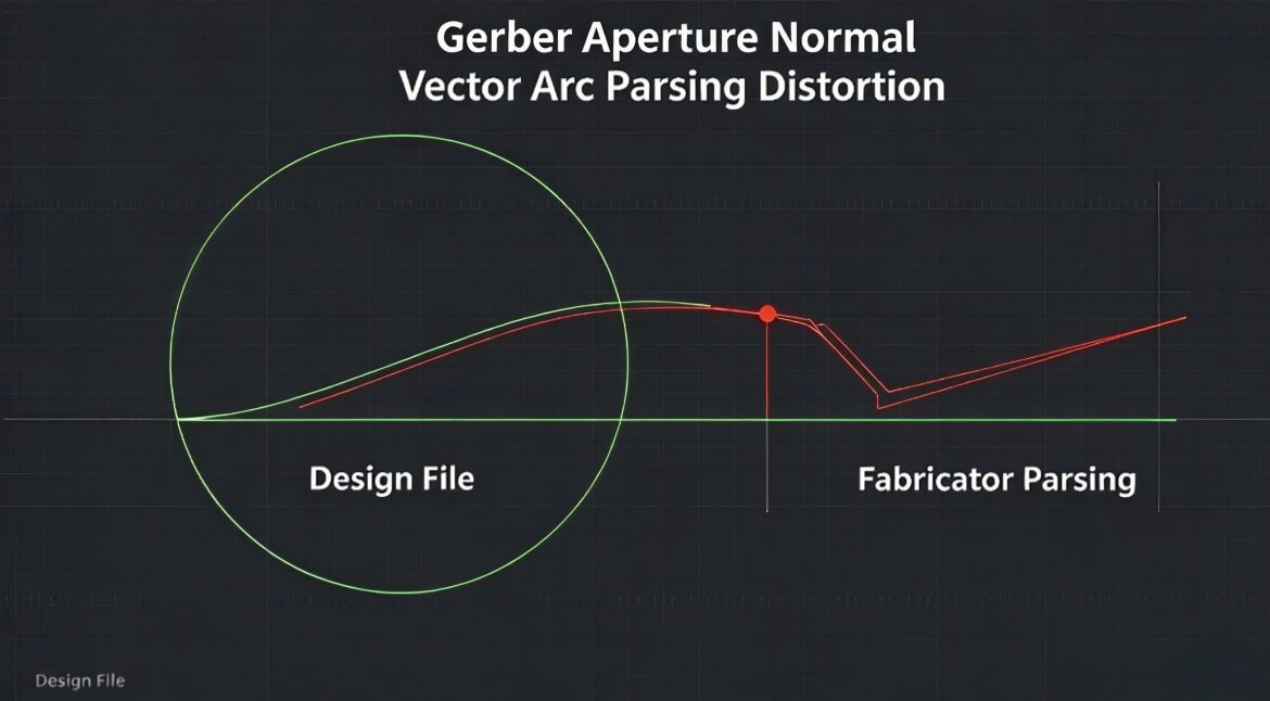
One potential source of this problem is the handling of a vector arc during CAM data preparation. Differences in arc interpolation, chordal tolerance, polygon conversion, compensation, and output processing can alter the final geometry used for imaging or etching.
This article explains how to identify and control these risks and how Kingda can help maintain geometric consistency from Gerber data to finished PCB.
A Typical Failure Scenario: Gerber Inspection Passes but Pads Shift
Consider a six-layer FR-4 PCB with ENIG surface treatment and a 0.3 mm-pitch QFN package.
The original Gerber file passes CAM inspection. Aperture definitions, D-code mapping, and G01/G02/G03 commands appear valid. However, after SMT assembly, AOI detects a large number of pads with positional deviations exceeding the customer’s specified tolerance.
If measurements show that the pad displacement is concentrated in a consistent direction rather than randomly distributed, the problem should not immediately be attributed to normal board expansion or shrinkage.
A systematic offset can indicate an issue somewhere in the manufacturing data chain, including:
- Gerber coordinate interpretation
- CAM software configuration
- Arc-to-line conversion
- Polygon reconstruction
- Image compensation
- Etching compensation
- Panelization or data transformation
- Registration between production layers
The key question is therefore:
Does the manufactured geometry still represent the original design geometry after CAM processing?
How a Vector Arc Can Be Changed During CAM Processing
Gerber data can represent circular geometry using arc commands such as G02 and G03. Depending on the CAM workflow, these arcs may be preserved as true arcs or converted into a series of short linear segments.
This conversion is not necessarily a manufacturing defect. In many production systems, linearization is a normal computational process. The critical factor is the accuracy with which the vector arc is reconstructed.
The relationship can be simplified as:
Gerber geometry → CAM interpretation → geometric conversion → compensation → imaging data → etching → finished PCB
Every transformation introduces an opportunity for geometric deviation.
Arc Interpolation and Chordal Tolerance
During arc interpolation, a curved path can be approximated by multiple straight-line segments. The maximum deviation between the original arc and the approximated path is commonly controlled by a parameter known as chordal tolerance or chord height tolerance.
A smaller tolerance produces more segments and generally provides a closer approximation to the original curve.
A larger tolerance reduces the number of segments but increases the maximum geometric deviation.
For example, a small-radius rounded pad corner requires substantially more linear segments than a large-radius arc when the same geometric tolerance is applied.
However, it is important not to assume that a particular tolerance value automatically produces a specific finished-pad displacement. The actual result depends on the CAM engine, compensation algorithm, data structure, imaging system, etching process, and board construction.
Therefore, a value such as 0.005 mm should be treated as a process-control requirement or qualification target, rather than a universal industry limit.
Why Linearization Can Affect Fine-Pitch PCB Features
For relatively large PCB features, small interpolation errors may have little practical impact.
The situation changes for fine-pitch components.
When the pad size, spacing, solder-mask opening, or rounded corner is very small, even a small geometric deviation can consume a meaningful portion of the available manufacturing tolerance.
Potential effects include:
- Pad center displacement
- Uneven rounded corners
- Non-uniform solder-mask openings
- Local line-width variation
- Irregular pad-to-pad spacing
- Reduced soldering margin
- AOI dimensional failures
The risk becomes more significant when several data-processing operations are performed sequentially.
For example:
Arc linearization → polygon conversion → compensation → scaling → imaging → etching
The individual errors do not necessarily add linearly, but repeated geometric transformations can create a measurable difference between the original design and the final production geometry.
Do Not Confuse CAM Parsing Errors With PCB Thermal Expansion
One important engineering distinction is the difference between data-processing errors and physical dimensional changes during PCB fabrication.
FR-4 laminates have different coefficients of thermal expansion in the X, Y, and Z directions. Laminate structure, resin content, glass style, copper distribution, temperature history, and board thickness all affect dimensional behavior.
However, material CTE should not automatically be used to explain a consistent pad offset that originates from CAM geometry.
If the original coordinate data is correct but the production CAM output contains a systematic geometric transformation, changing laminate CTE will not solve the underlying data-processing problem.
A practical failure analysis should therefore separate the problem into two categories:
- Geometric data deviation — caused by data interpretation, conversion, scaling, compensation, or output processing.
- Physical dimensional deviation — caused by material expansion, shrinkage, registration, lamination, etching, or other manufacturing effects.
This distinction can significantly shorten the troubleshooting process.
Three Steps to Identify a Vector Arc Parsing Problem
Step 1: Inspect the Gerber Commands
Open the original Gerber file with an appropriate text editor or Gerber viewer and search for G02 and G03 commands.
Identify which layers contain arc geometry, such as:
- Top copper
- Bottom copper
- Solder mask
- Fine-pitch component pads
- Rounded slots or mechanical features
Do not rely only on the presence of G02/G03 commands. The complete coordinate structure and aperture definitions must also be evaluated.
The purpose of this inspection is to determine whether the original design actually contains true arc information or whether the geometry has already been converted into short line segments by the EDA export process.
Step 2: Compare CAM Input and CAM Output
Load the original data into the production CAM software and compare the geometry before and after processing.
Pay particular attention to:
- Arc interpolation settings
- Chordal tolerance
- Polygon conversion
- Scaling factors
- Image compensation
- Etching compensation
- Coordinate transformations
- Aperture replacement
- Region reconstruction
If the CAM system provides a preview of the processed geometry, compare the pad center, radius, edge profile, and relative position against the original design.
A useful verification method is to overlay the original Gerber geometry with the final imaging data and measure the maximum deviation.
Step 3: Inspect the Finished PCB
If the discrepancy remains after CAM verification, inspect the physical PCB.
Measure:
- Pad center coordinates
- Pad-to-pad pitch
- Pad diameter or length/width
- Solder-mask opening
- Layer-to-layer registration
- Etched edge profile
- Overall board dimensions
A microscopic or optical inspection can also determine whether a curved edge has been reproduced smoothly or appears segmented.
However, a visibly stepped edge alone should not be treated as absolute proof of CAM linearization. Imaging resolution, etching behavior, inspection magnification, and feature geometry can produce similar visual effects.
Engineering Control: Define Arc Processing Requirements
For customers using fine-pitch packages, geometric processing requirements should be included in the PCB manufacturing specification rather than left entirely to default CAM settings.
A technical agreement can define:
- Required geometric accuracy
- Maximum permitted interpolation deviation
- Required treatment of G02/G03 data
- Acceptable polygon approximation
- Scaling accuracy
- Compensation methodology
- Verification method
- Production approval criteria
Instead of simply specifying that the manufacturer must use a particular default value, it is more effective to define the required output accuracy and verification method.
This allows the manufacturer to achieve the requirement using its actual CAM and production equipment.
Avoid Relying on CAM Defaults
CAM systems may have different default configurations for arc processing and polygon handling.
Two manufacturers can receive identical Gerber data but generate slightly different intermediate production data because their CAM workflows are configured differently.
For critical products, Kingda recommends documenting important CAM parameters during engineering review and validating them against the customer’s dimensional requirements.
Particular attention should be given to:
- CAM software version and processing method
- Arc interpolation settings
- Chordal tolerance
- Gerber format configuration
- Polygon and region handling
- Scaling and compensation
- Output format
- Imaging equipment resolution
The objective is not simply to make the CAM configuration more conservative. It is to establish a controlled and repeatable data-processing chain.
Solder Mask Geometry Requires Special Attention
Solder-mask openings are another area where curved geometry can become sensitive.
For very small pads, a combination of pad dimensions, mask expansion, corner radius, and manufacturing registration can affect the final opening.
Where the design allows it, standardized pad geometries can simplify CAM processing.
For example, a rounded-rectangle pad defined through a controlled aperture or region structure may be easier to reproduce consistently than a complex collection of small vector segments.
However, the preferred data structure depends on the EDA tool, Gerber export settings, CAM system, and manufacturer’s process capability.
Therefore, designers should validate the complete data path rather than assuming that one geometry format is universally superior.
The Altium Gerber Export Trap
EDA export settings can also influence the final geometry.
For example, when polygon or region data is exported, different settings may cause the geometry to be represented as:
- A true region
- Multiple vector segments
- An aperture-based shape
- A combination of regions and apertures
If a complex pad or copper region is converted into a large number of short line segments before reaching the PCB manufacturer, the original geometric intent may already be lost.
This is why the first troubleshooting step should always be to compare the exported Gerber geometry with the source PCB design.
The question is not simply whether the Gerber file is “valid.”
The more important question is whether the Gerber file accurately represents the intended manufacturing geometry.
Why ENIG and Etching Must Be Considered Separately
ENIG surface finishing and copper etching can influence the final dimensions of PCB features, but they should not automatically be connected to a CAM arc-parsing problem.
During copper processing, line edges can be affected by:
- Copper thickness
- Etchant chemistry
- Etching rate
- Line width
- Aspect ratio
- Process temperature
- Conveyor speed
- Resist profile
ENIG introduces additional surface-finishing steps after copper pattern formation.
Therefore, if a pad is already geometrically displaced in the imaging data, ENIG is not the original cause. If the geometry is correct before etching but becomes distorted afterward, the investigation should focus on the wet-process and dimensional-control stages.
This stage-by-stage separation is essential for accurate root-cause analysis.
High-Frequency Materials Need a Different Verification Approach
High-frequency PCBs introduce additional material and dimensional considerations.
Materials such as Rogers laminates have different dielectric properties, thermal expansion characteristics, copper foil structures, and processing requirements compared with conventional FR-4.
For high-frequency designs, dimensional accuracy is important not only for pad geometry but also for:
- Controlled impedance
- Differential-pair spacing
- Trace width
- Reference-plane spacing
- Via transitions
- RF structures
Nevertheless, material CTE should be evaluated independently from CAM interpolation accuracy.
A CAM geometric error is a data-processing issue, while temperature-induced dimensional change is a physical manufacturing and operating-condition issue. Combining the two without measurement can lead to an incorrect root-cause conclusion.
Do Not Use a General Pad Tolerance as the Only Acceptance Criterion
Another common mistake is using a general PCB dimensional tolerance as the sole acceptance criterion for a specialized fine-pitch feature.
A general manufacturing tolerance may not adequately describe:
- CAM geometric conversion accuracy
- Pad-center position
- Solder-mask opening accuracy
- Fine-pitch registration
- Arc reconstruction accuracy
- Local feature-to-feature accuracy
For demanding applications, the manufacturing specification should define the critical dimensions separately.
A dedicated verification structure can also be added to the PCB panel.
For example, a test coupon may contain:
- Concentric circular patterns
- Fine-pitch pad arrays
- Rounded pads
- Arc-to-line transition structures
- Registration targets
- Known reference coordinates
The measured result can then be compared with the original Gerber coordinates and CAM output.
A More Reliable Verification Workflow
For critical PCB projects, a closed-loop verification process is more reliable than checking only the original Gerber file.
A practical workflow is:
EDA design
↓
Gerber export
↓
Gerber file verification
↓
CAM import
↓
CAM geometry comparison
↓
Production data output
↓
Imaging
↓
Etching
↓
Finished PCB dimensional inspection
At each stage, engineers should maintain a measurable reference.
If the geometry changes between two stages, the investigation can focus on the transformation that occurred between those stages.
This approach is much more effective than simply repeating the CAM export or changing material parameters without identifying the actual source of deviation.
Practical Design and Manufacturing Recommendations
To reduce the risk of geometric distortion in fine-pitch PCB manufacturing, designers and manufacturers can follow several practical rules:
- Use a validated Gerber export configuration.
- Verify critical G02/G03 geometry before manufacturing.
- Avoid unnecessary conversion of arcs into short vector segments.
- Document chordal tolerance requirements for critical curved features.
- Compare CAM input and output for high-risk pads.
- Verify scaling and coordinate transformations.
- Inspect solder-mask openings separately from copper pads.
- Use production-representative test coupons for critical dimensions.
- Separate CAM errors from material expansion and etching effects.
- Establish measurable acceptance criteria with the PCB manufacturer.
These controls are particularly useful for QFN, BGA, RF, HDI, and other high-density PCB applications.
How Kingda Controls Gerber Geometry and Manufacturing Accuracy
At Kingda, PCB manufacturing quality begins before the first production panel enters the line.
Our engineering process can review customer Gerber data, identify critical geometries, evaluate CAM processing requirements, and verify whether the manufacturing data remains consistent with the original design intent.
For fine-pitch and high-density PCB projects, particular attention can be given to:
- Gerber file integrity
- Vector arc processing
- CAM software configuration
- Arc interpolation
- Chordal tolerance
- Pad and solder-mask geometry
- Layer registration
- Etching compensation
- Finished-board dimensional inspection
Rather than relying on a single inspection point, the goal is to maintain geometric consistency throughout the complete PCB manufacturing process.
For customers with strict dimensional requirements, Kingda can also work with the engineering team to define inspection structures and acceptance criteria before mass production.
Conclusion
A Gerber file passing a standard CAM check does not necessarily guarantee that every geometric feature will be reproduced exactly as intended on the finished PCB.
For fine-pitch designs, vector arc processing deserves particular attention because different CAM software systems may handle arc interpolation, polygon conversion, and compensation differently.
The most effective approach is to establish a controlled data chain from EDA design through Gerber file generation, CAM processing, imaging, etching, and final inspection.
By controlling arc interpolation, defining an appropriate chordal tolerance, and comparing intermediate manufacturing data with the original design, engineers can identify geometric deviations before they become SMT or AOI failures.
For high-density PCB applications, early engineering verification and clear manufacturing specifications are essential to achieving consistent pad accuracy and production reliability.