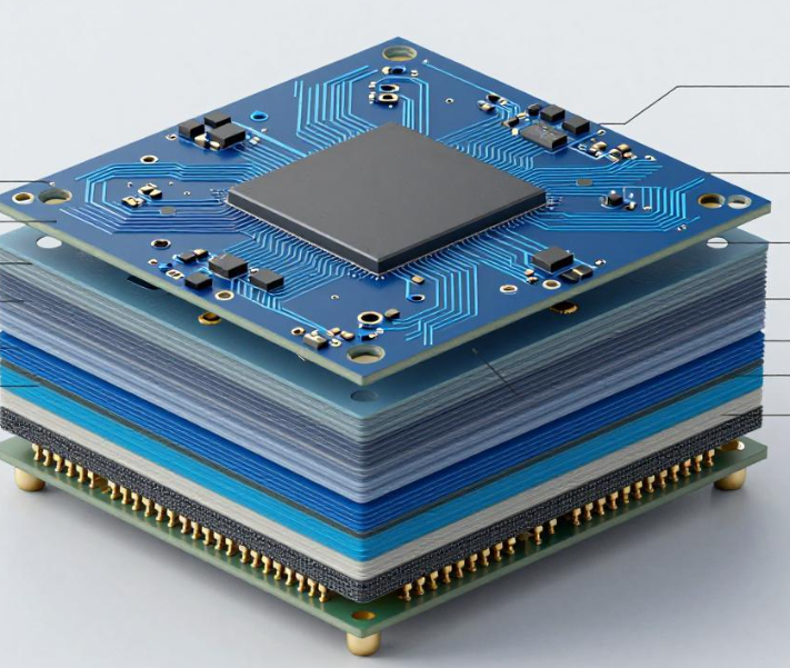
When engineers calculate dielectric thickness in a multilayer PCB stackup, the primary focus is often target impedance. However, the physical topography created by etched inner-layer copper is equally important.
After inner-layer etching, copper-covered areas and resin-filled areas do not have the same surface height. During lamination, the resin in prepreg must flow into and around these topographical differences. If the stackup is designed without considering the actual copper distribution, engineers may select more prepreg than the process really requires.
A more refined approach combines PCB stackup optimization with an evaluation of inner-layer copper distribution and copper thickness. Instead of automatically selecting high-resin-content or thick PP materials, engineers can evaluate the actual filling requirements and determine an appropriate dielectric construction.
This approach can reduce material consumption while maintaining impedance control, lamination quality, and long-term reliability.
How Inner-Layer Copper Affects Prepreg Selection
In a multilayer PCB, inner-layer cores are patterned through imaging and etching before lamination. The remaining copper creates raised areas, while regions without copper expose the underlying dielectric.
The resulting surface profile depends on several factors, including:
- Copper thickness
- Copper coverage
- Trace density
- Large copper pours
- Plane structures
- Clearance patterns
- Local copper distribution
- Prepreg resin content
- Lamination pressure and temperature
The purpose of PP thickness selection is not simply to fill the largest theoretical gap. It must provide sufficient resin flow and dielectric thickness after lamination while remaining compatible with the required electrical and mechanical characteristics.
If the inner layer contains relatively sparse routing and limited copper coverage, the copper-induced topography may be less demanding than a dense or heavy-copper plane layer.
Conversely, heavy copper and large continuous copper areas can create more significant local height differences and require careful consideration of resin flow and final dielectric thickness.
Therefore, using the same high-resin-content PP construction for every stackup may create unnecessary material and process costs.
Understanding Copper Thickness Compensation
The concept of copper thickness compensation is based on the physical relationship between inner-layer copper and the dielectric material surrounding it.
When an inner layer contains thicker copper, that copper occupies physical space within the stackup. During lamination, the prepreg resin flows around the copper features and fills the remaining spaces between adjacent layers.
Consequently, inner layer copper should be included in stackup calculations rather than treating the copper pattern as an electrically important feature only.
A practical stackup evaluation should consider:
- Finished copper thickness
- Copper coverage percentage
- Copper pattern distribution
- Trace and plane geometry
- Prepreg resin content
- Lamination flow behavior
- Final dielectric thickness
- Required impedance
This does not mean that thicker copper always allows the same amount of prepreg to be removed. The actual relationship depends on the copper pattern, prepreg system, lamination conditions, target dielectric thickness, and manufacturer process capability.
The correct objective is to determine the minimum practical dielectric construction that still provides adequate resin filling and meets the electrical and mechanical requirements.
Copper Distribution Matters More Than Average Copper Area
Average copper coverage is useful for initial analysis, but it does not fully describe the actual lamination challenge.
Two inner layers may both have 60% copper coverage while having completely different layouts.
For example, one layer may contain evenly distributed narrow traces, while another may contain a large solid copper region surrounded by large open areas. Their local topography and resin-flow behavior can therefore be different.
This is why copper distribution should be evaluated spatially rather than using only a single percentage.
Important areas to examine include:
- Large copper planes
- Large copper-free regions
- Dense routing zones
- Heavy-copper regions
- Narrow copper necks
- Isolated copper areas
- Transition areas between high- and low-copper-density regions
A detailed copper-density map can help identify areas where the selected prepreg construction may require additional process validation.
Optimize the Stackup Together With Inner-Layer Layout
Reducing prepreg consumption should not be achieved simply by selecting a thinner material. The inner-layer layout itself can sometimes be optimized to make the lamination structure more uniform.
For example, where electrical requirements permit, large isolated copper blocks can be redistributed or modified to improve copper balance.
Large copper areas may also be designed with appropriate patterns or structures that promote more uniform copper distribution. However, this approach must be used carefully.
A copper mesh or patterned plane can alter:
- DC resistance
- Current-carrying capability
- Plane impedance
- Power distribution
- High-frequency return paths
- Electromagnetic behavior
Therefore, PCB stackup optimization and copper-pattern optimization must remain consistent with the electrical design.
A power plane should never be converted into a mesh merely to reduce prepreg requirements without verifying its electrical performance.
For high-current or high-speed designs, power integrity and signal integrity should be checked before and after any significant change to the copper pattern.
Prepreg Selection Should Be Based on Actual Lamination Requirements
Prepreg selection involves more than nominal thickness.
Different PP styles can have different resin contents, flow characteristics, cured dielectric thicknesses, and behavior under specific lamination conditions.
When optimizing prepreg selection, engineers should evaluate:
- Nominal PP thickness
- Resin content
- Resin flow
- Glass style
- Cured dielectric thickness
- Copper topography
- Lamination pressure
- Lamination temperature
- Heating and cooling profile
- Required impedance
The final dielectric thickness after lamination is influenced by both the PP construction and the amount of resin consumed during flow.
Therefore, a PP datasheet value should not automatically be interpreted as the final dielectric thickness between two copper layers.
For controlled-impedance boards, the actual cured dielectric thickness and dielectric properties should be used in the impedance model.
Example of a Six-Layer Stackup Optimization
Consider a six-layer PCB using relatively heavy copper on one or more inner layers.
An initial stackup may use two high-resin-content PP sheets simply because the design team wants to ensure sufficient filling around the copper features.
After reviewing the actual copper distribution, engineers may find that the copper topography is more uniform than originally assumed. A different PP combination may then provide sufficient resin flow while achieving the required final dielectric thickness.
The revised design should be evaluated through:
- Lamination simulation or process assessment
- Prepreg flow analysis
- Cross-section inspection
- Final dielectric-thickness measurement
- Impedance simulation
- Test-coupon verification where required
The important point is that the alternative PP construction should be selected based on the actual stackup and manufacturing process, rather than assuming that a thinner PP is automatically better.
Verify Lamination Process Capability
Reducing PP thickness or resin content changes the lamination process window. This makes process validation essential.
After stackup optimization, engineers should check whether the revised construction provides sufficient resin to completely fill the required spaces.
Cross-section analysis should examine:
- Voids
- Resin starvation
- Incomplete filling
- Delamination
- Copper-to-resin interfaces
- Dielectric thickness variation
- Inner-layer registration
- Glass/resin distribution
A small pilot run is often useful when a stackup is substantially different from a manufacturer’s established construction.
The lamination cycle may need to be reviewed based on heating rate, pressure application, vacuum conditions, temperature profile, and cooling behavior.
The objective is to reduce unnecessary material without narrowing the manufacturing process window to an unacceptable level.
Impedance Control Must Be Recalculated After Stackup Changes
One important risk of stackup optimization is changing the dielectric geometry without updating the impedance model.
For controlled-impedance designs, impedance depends on multiple variables, including:
- Trace width
- Trace thickness
- Dielectric thickness
- Dielectric constant
- Trace-to-plane spacing
- Copper surface geometry
- Differential-pair spacing
- Frequency and modeling method
When PP thickness changes, the distance between a signal trace and its reference plane can also change.
Therefore, any significant stackup change should trigger a new impedance calculation.
For high-speed boards, the updated stackup should be reviewed using the actual material data and manufacturing tolerances. Where necessary, impedance coupons and TDR measurements can be used to verify production results.
This ensures that material-cost optimization does not unintentionally create impedance deviations.
Copper Balance and Board Warpage
Copper distribution also affects mechanical behavior during lamination.
When copper is heavily concentrated on one side of a multilayer structure, the resulting imbalance can contribute to dimensional instability or board warpage.
A well-designed stackup should therefore consider copper balance across the entire board rather than optimizing one layer independently.
Useful checks include:
- Copper area by layer
- Symmetry between corresponding layers
- Heavy-copper locations
- Large copper-free regions
- Core and prepreg construction
- Overall board thickness
- Expected lamination shrinkage
Good multilayer PCB design balances electrical performance, mechanical stability, manufacturability, and cost.
Do Not Optimize Material Cost at the Expense of Reliability
The goal of reducing PP consumption is not to use the smallest possible dielectric thickness.
If insufficient resin is available for proper filling, the resulting defects can include voids, resin starvation, poor interlayer bonding, and increased delamination risk.
These defects may not be visible during initial electrical testing but can become significant during thermal cycling, humidity exposure, or long-term operation.
For high-reliability applications, stackup optimization should therefore be evaluated against the complete reliability requirement.
The correct sequence is:
Copper distribution analysis → stackup simulation → PP selection → lamination validation → impedance verification → reliability evaluation.
This approach is more reliable than simply replacing a thick PP with a thinner one based on nominal dimensions.
A Practical Workflow for PCB Stackup Optimization
A production-oriented workflow can be organized into the following steps:
Step 1: Analyze Inner-Layer Copper
Generate copper-density information for every inner layer and identify areas with significant local copper variation.
Step 2: Review Copper Thickness
Record the actual finished copper thickness rather than relying only on nominal foil designations.
Step 3: Evaluate Surface Topography
Consider how the copper pattern changes the physical height profile between adjacent layers.
Step 4: Select Candidate Prepreg Constructions
Compare different PP styles based on resin content, cured thickness, flow characteristics, and manufacturer process capability.
Step 5: Recalculate the Stackup
Update the complete stackup model and confirm final board thickness, dielectric thickness, and mechanical symmetry.
Step 6: Recalculate Impedance
Update single-ended and differential impedance models using the revised dielectric geometry and material properties.
Step 7: Validate Lamination
Use pilot production, cross-section analysis, or other appropriate process-validation methods to confirm resin filling and interlayer bonding.
Step 8: Verify Reliability
For demanding applications, perform the appropriate thermal, humidity, insulation, mechanical, and reliability testing.
This workflow allows material reduction to be treated as an engineering optimization rather than a simple purchasing decision.
Kingda’s Multilayer PCB Stackup Optimization
Kingda can support customers with multilayer PCB stackup development and manufacturing-oriented optimization.
Our engineering evaluation can consider inner-layer copper distribution, copper thickness, dielectric construction, prepreg selection, impedance requirements, lamination conditions, and manufacturing tolerances.
Rather than selecting PP based only on nominal thickness, the stackup can be evaluated against the actual PCB structure and production process.
This integrated approach helps balance material utilization, impedance control, lamination quality, board reliability, and manufacturing cost.
Conclusion
Inner-layer copper is an important part of multilayer stackup design and should not be ignored when selecting dielectric materials.
By analyzing inner layer copper, evaluating copper distribution, and incorporating copper thickness into the stackup model, engineers can determine whether the selected prepreg construction is providing more resin and dielectric thickness than the design actually requires.
However, reducing PP thickness should always be supported by lamination validation and impedance recalculation. Copper-pattern optimization must also consider power integrity, signal integrity, thermal performance, and mechanical stability.
A well-executed PCB stackup optimization process does more than reduce material consumption. It creates a better balance between manufacturing cost, electrical performance, lamination reliability, and production consistency.