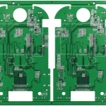
Medical monitoring equipment places demanding requirements on PCB reliability, especially when the electronic system is used for long-term physiological signal acquisition or operates near the human body.
A 4-layer PCB may pass functional testing immediately after assembly while still containing latent material, contamination, insulation, or interconnection risks that only become apparent after prolonged environmental exposure.
For this reason, PCB reliability testing should be considered during product development rather than treated as a final inspection step.
Depending on the product architecture, applicable standards, intended environment, and regulatory requirements, reliability verification may include temperature cycling, humidity exposure, insulation testing, thermal stress, solderability, and other application-specific tests.
The objective is to identify potential failure mechanisms before they affect the complete medical monitoring system.
Why Functional Testing Alone Is Not Enough
A prototype can power on correctly, acquire ECG or other physiological signals, and pass short-duration functional testing while still having long-term reliability weaknesses.
Some PCB-related failure mechanisms develop gradually under environmental stress, including:
- Moisture absorption
- Ionic contamination
- Insulation resistance degradation
- Electrochemical migration
- Delamination
- Copper cracking
- Solder-mask degradation
- Interlayer bonding problems
- Leakage current increase
These issues are particularly important in high-impedance analog acquisition circuits.
When moisture and contamination create an unintended conductive path between adjacent conductors, even a relatively small leakage current can influence a sensitive measurement circuit.
Therefore, the functional performance of a medical PCB should be evaluated together with its environmental and electrical reliability.
Case Background: Four-Layer PCB for Wearable Monitoring
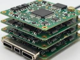
In one representative development scenario, a wearable monitoring device used a four-layer PCB for physiological signal acquisition.
The prototype completed functional debugging successfully. However, during environmental reliability verification, some samples exhibited a gradual reduction in input insulation resistance and measurable baseline drift after prolonged high-temperature and high-humidity exposure.
The investigation excluded the primary electronic components as the dominant failure source. Attention then shifted to the PCB itself.
The analysis identified several potential contributing mechanisms:
- Moisture absorption by the dielectric material
- Surface ionic contamination
- Increased leakage around high-impedance acquisition nodes
- Insufficient insulation margin in sensitive areas
- Environmental exposure of vulnerable PCB surfaces
This type of failure demonstrates why PCB reliability testing needs to examine both materials and manufacturing processes.
Key Reliability Tests for Medical Monitoring PCBs
The exact qualification program should be determined by the product requirements and applicable standards. However, several categories are particularly relevant when evaluating a 4-layer PCB for demanding monitoring applications.
Temperature Cycling
Temperature cycling exposes the PCB to repeated expansion and contraction.
A representative development test may use a temperature range such as -40°C to 85°C for a defined number of cycles. The actual temperature limits, dwell time, transition rate, and cycle count should be established according to the product’s operating environment and qualification plan.
Temperature cycling can help reveal:
- Interlayer delamination
- Copper fatigue
- Via reliability problems
- Solder-joint degradation
- Material-interface stress
- Mechanical deformation
Different materials have different coefficients of thermal expansion (CTE). Repeated thermal excursions can therefore generate mechanical stress between copper, resin, glass reinforcement, components, and other structures.
Humidity and Temperature Testing
Humidity exposure is especially important for sensitive analog and high-impedance circuits.
A commonly used accelerated condition in reliability programs is 85°C/85% relative humidity, often referred to as an 85/85 test. The duration depends on the applicable qualification requirement; a 1,000-hour exposure can be used as a project-specific validation condition.
The test can help evaluate:
- Moisture absorption
- Insulation resistance
- Ionic contamination sensitivity
- Electrochemical migration
- Delamination
- Surface insulation behavior
- Long-term material stability
The purpose is not simply to determine whether the PCB continues to function after exposure. Electrical parameters should also be monitored to identify gradual degradation.
Insulation Resistance Is Critical in High-Impedance Circuits
For physiological signal acquisition, the input impedance of the analog front end can be relatively high.
Under these conditions, unintended leakage paths that would be insignificant in a low-impedance power circuit may become important.
Potential leakage paths can develop through:
- PCB surface contamination
- Moisture films
- Solder-mask defects
- Residual ionic materials
- Inadequate conductor spacing
- Contaminated connectors
- Material interfaces
Therefore, insulation resistance should be monitored under appropriate environmental and electrical conditions.
The measurement method and acceptance criteria should be defined according to the circuit design and applicable product requirements rather than using one universal resistance value.
Ionic Contamination and Electrochemical Migration
Ionic contamination is another important reliability consideration.
Residues from PCB fabrication, handling, assembly, cleaning chemicals, flux, or other process materials may contain ionic species. Under elevated humidity and electrical bias, these residues can contribute to surface leakage and, under suitable conditions, electrochemical migration.
For high-impedance monitoring circuits, even small leakage paths can influence signal measurements.
A reliability-oriented manufacturing process should therefore control:
- Cleaning effectiveness
- Chemical residues
- Handling contamination
- Surface cleanliness
- Solder-mask integrity
- Storage conditions
- Environmental exposure
Where required, ionic cleanliness can be evaluated using an appropriate test method and acceptance criterion.
Material Selection for Moisture Reliability
Material selection is an important part of medical PCB reliability.
Standard FR-4 materials can cover a wide range of applications, but different material systems have different moisture absorption, thermal, electrical, and mechanical characteristics.
For demanding monitoring applications, engineers may evaluate materials according to:
- Moisture absorption
- Tg
- Td
- CTE
- Dielectric properties
- Df
- Thermal stability
- CAF resistance
- Insulation characteristics
A lower-moisture-absorption material may provide advantages in applications where environmental humidity has a significant effect on electrical insulation.
However, material selection should be based on the complete stackup and qualification requirements rather than assuming that one material property alone determines PCB reliability.
Improve PCB Cleaning and Surface Cleanliness
When contamination is identified as a potential contributor to leakage, the manufacturing process should be reviewed in addition to the material selection.
Cleaning parameters should be evaluated according to the actual PCB surface finish, solder mask, component population, chemistry, and assembly process.
Possible controls include:
- Optimizing post-process cleaning
- Controlling cleaning chemistry
- Verifying rinse quality
- Improving drying conditions
- Reducing handling contamination
- Establishing cleanliness inspection procedures
Plasma treatment may be useful for certain surface-preparation applications, but it should not automatically be treated as a substitute for an appropriately controlled cleaning process.
The selected process should be validated for the specific PCB structure and contamination mechanism.
Protect High-Impedance Acquisition Areas
Sensitive acquisition areas deserve additional layout attention.
The PCB design should consider:
- Adequate conductor spacing
- Controlled leakage paths
- Guarding where appropriate
- Clean routing around sensitive nodes
- Appropriate solder-mask coverage
- Separation from noisy power circuits
- Connector and electrode interface geometry
Increasing the spacing between conductors can increase insulation margin, but the required spacing depends on voltage, environment, applicable safety requirements, PCB material, contamination level, and geometry.
For electrode interfaces and other patient-connected circuits, the PCB design must also be evaluated as part of the complete electrical safety architecture.
Solder Mask Quality Matters
Solder mask is not merely a cosmetic coating.
In sensitive areas, defects such as pinholes, insufficient coverage, contamination, or poor adhesion can create additional leakage or environmental-exposure paths.
During reliability evaluation, the solder-mask system should therefore be reviewed for:
- Coverage
- Adhesion
- Surface defects
- Chemical resistance
- Moisture resistance
- Compatibility with cleaning processes
Where a sensitive conductor is dependent on solder-mask coverage for environmental protection, the design and manufacturing process should provide appropriate margin.
Four-Layer Stackup and Reliability Considerations
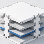
A 4-layer PCB often uses a structure such as signal-ground-power-signal or another application-specific arrangement.
The selected stackup affects more than signal integrity.
It can also influence:
- Board thickness
- Thermal expansion
- Mechanical symmetry
- Impedance
- Power distribution
- Via structures
- Dielectric thickness
- Moisture-related insulation behavior
A balanced stackup can help control mechanical deformation, while appropriate dielectric selection can support the required electrical and environmental performance.
For sensitive monitoring products, stackup development should therefore consider electrical performance and reliability at the same time.
Reliability Verification After Corrective Actions
After identifying a PCB-related failure mechanism, corrective actions should be verified systematically.
A representative improvement program may include:
Material Optimization
Evaluate a material system with appropriate moisture, thermal, and electrical characteristics for the intended application.
Manufacturing Process Optimization
Review cleaning, handling, drying, solder-mask processing, and other operations that may influence ionic contamination or surface insulation.
Layout Optimization
Increase insulation margin where appropriate and improve separation around high-impedance acquisition nodes.
Environmental Protection
Depending on the product architecture, conformal coating or another protective system may be considered to reduce environmental exposure.
The coating material and process must themselves be evaluated for compatibility with connectors, electrodes, components, rework requirements, and electrical safety.
Repeat the Environmental Reliability Test
After corrective actions, the revised PCB should undergo the relevant qualification tests again.
For a project using an 85°C/85% RH, 1,000-hour condition as its development requirement, measurements should be taken before, during, and after the exposure where practical.
Important parameters may include:
- Insulation resistance
- Leakage current
- Signal baseline stability
- Functional performance
- Physical delamination
- Surface condition
- Interlayer integrity
The objective is to confirm that the corrective action addresses the underlying failure mechanism rather than simply restoring short-term functionality.
Build Reliability Into the Design Stage
The most effective reliability strategy is to identify potential failure mechanisms before the PCB reaches formal product qualification.
During early development, engineers should establish a reliability checklist covering:
- Material selection
- Stackup construction
- Copper thickness
- Conductor spacing
- Surface cleanliness
- Solder-mask design
- High-impedance routing
- Environmental exposure
- Electrical insulation
- Manufacturing process controls
This allows reliability requirements to influence the PCB design before tooling and mass production are finalized.
It is generally much more efficient to correct a layout or material-selection issue during engineering development than after a complete system-level qualification test has failed.

Reliability Testing Should Match the Actual Product
It is important to distinguish between a development example and a universal qualification requirement.
A wearable monitoring product, bedside monitor, implant-related system, and industrial physiological sensor may have very different electrical, environmental, and regulatory requirements.
Therefore, the reliability program should be established according to:
- Intended use
- Patient-contact architecture
- Operating environment
- Expected service life
- Electrical safety requirements
- Applicable medical-device standards
- Customer qualification specifications
- Manufacturing process
This approach prevents engineers from applying a generic test matrix without considering the actual risk profile of the product.
Kingda’s Medical PCB Manufacturing Support
Kingda supports the development and manufacturing of medical PCB solutions, including four-layer boards for demanding electronic applications.
Our engineering-oriented approach can consider material selection, stackup design, copper distribution, impedance requirements, surface cleanliness, fabrication tolerances, and reliability-related manufacturing controls.
For sensitive monitoring applications, the PCB should be evaluated as part of the complete electronic system rather than as an isolated circuit board.
By identifying potential environmental and manufacturing risks during development, Kingda helps customers establish a more controlled transition from prototype validation to production.
Conclusion
The reliability of a 4-layer PCB used in life-monitoring equipment cannot be confirmed through short-duration functional testing alone.
Environmental exposure can reveal failure mechanisms related to moisture absorption, ionic contamination, insulation degradation, material interfaces, and manufacturing residues.
A comprehensive PCB reliability testing program should therefore combine appropriate environmental, electrical, mechanical, and process-related verification.
For sensitive medical PCB applications, material selection, stackup design, conductor spacing, surface cleanliness, solder-mask quality, and manufacturing process control all contribute to long-term reliability.
The most effective strategy is to identify these risks during PCB development, validate corrective actions through appropriate testing, and establish manufacturing controls before mass production begins.
For medical monitoring products, reliability is not simply a final test result. It is the outcome of coordinated design, material selection, manufacturing control, and application-specific validation.