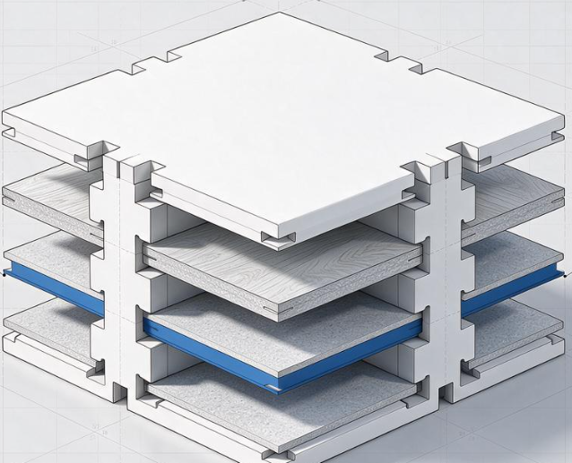
In the total cost structure of a multilayer PCB, prepreg (PP) can represent a significant portion of the raw-material cost, particularly for high-layer-count, large-format, and high-volume production.
The selection of PP materials and the overall stackup directly affect material utilization, lamination performance, dielectric thickness, impedance, and production cost.
Many hardware engineers focus primarily on impedance and electrical performance when developing a stackup, while giving less attention to whether the selected PP construction contains unnecessary thickness or resin content.
Selecting a thicker PP than necessary, using excessive resin content, or combining multiple PP sheets simply to reach a target thickness can increase material consumption and manufacturing complexity.
A well-designed multilayer PCB stackup should therefore balance electrical requirements, mechanical performance, manufacturing capability, material availability, and cost.
The objective is not simply to use less PP. It is to eliminate unnecessary material while maintaining the required electrical, mechanical, thermal, and reliability performance.
The Role of Prepreg in Multilayer PCB Manufacturing
Prepreg, short for pre-impregnated material, is typically composed of glass reinforcement impregnated with partially cured resin.
During PCB lamination, heat and pressure cause the resin system to flow and cure, bonding the inner-layer cores and copper foils into a multilayer structure.
PP serves several important functions:
- Bonds adjacent PCB layers
- Fills spaces around inner-layer copper features
- Contributes to the final dielectric thickness
- Helps establish signal-to-reference-plane spacing
- Influences controlled impedance
- Contributes to mechanical strength and dimensional stability
PP materials are available in different glass styles, resin contents, nominal thicknesses, and flow characteristics.
Therefore, selecting PP should not be treated as a simple thickness-matching exercise.
The selected construction must work with the actual copper pattern, lamination process, board thickness, impedance requirements, and manufacturing tolerances.
Where PP Material Waste Commonly Comes From
PP-related waste in multilayer PCB production generally comes from several sources.
Excessive Dielectric Thickness
One common issue is adding excessive dielectric thickness as a safety margin.
For example, an engineer may determine that a specific signal layer requires a certain dielectric geometry for impedance control, but then select a substantially thicker PP construction simply because it is readily available.
A larger dielectric thickness can change the impedance relationship between the trace and its reference plane. It may also increase overall board thickness and material consumption.
The appropriate dielectric thickness should therefore be determined through impedance modeling and stackup analysis rather than arbitrary safety margins.
Multiple PP Sheets for One Dielectric Layer
Another source of waste occurs when two or more thin PP sheets are combined to approximate a required dielectric thickness.
This approach can be technically appropriate when no suitable single-sheet construction exists. However, if a standard single PP construction can achieve the required final dielectric thickness, unnecessary stacking may increase cutting, handling, inventory, and process complexity.
The decision should therefore be based on the actual material library and lamination capability of the selected PCB manufacturer.
Excessive Resin Content
Using a high-resin-content PP for every dielectric layer is another potential source of unnecessary cost.
High-resin-content materials can be useful when significant copper topography needs to be filled. However, they are not automatically required for every layer.
For layers with relatively uniform copper distribution and limited topographical variation, another PP construction may provide sufficient bonding and dielectric performance.
Use Impedance Modeling to Determine the Required Dielectric Structure
The first step in prepreg selection should be to establish the required final dielectric geometry.
For controlled-impedance PCB designs, the relationship between trace geometry and the surrounding dielectric structure must be considered.
Important variables include:
- Trace width
- Finished copper thickness
- Trace-to-plane distance
- Dielectric constant
- Differential-pair spacing
- Copper surface geometry
- Frequency
- Manufacturing tolerances
Instead of selecting PP based solely on nominal thickness, engineers should first determine the required cured dielectric thickness and then identify material constructions capable of achieving it.
This approach helps eliminate unnecessary dielectric thickness while keeping the electrical design within its specified impedance range.
PP Nominal Thickness Is Not the Same as Final Thickness
A critical point in PCB lamination is that the nominal thickness of a PP sheet should not be assumed to equal its final thickness after lamination.
During the lamination cycle, resin flows into spaces around copper features and the glass-resin structure is compressed.
The final dielectric thickness is affected by:
- Glass style
- Resin content
- Copper thickness
- Copper coverage
- Copper distribution
- Lamination pressure
- Lamination temperature
- Resin flow characteristics
- Adjacent layer construction
Therefore, the final stackup should be developed using manufacturer-specific cured-thickness data whenever available.
This is especially important for controlled-impedance applications.
Example: Replacing Multiple PP Sheets With a Single Construction
Consider a four-layer PCB where the target dielectric construction between a signal layer and its reference plane is approximately 0.14 mm.
An initial design might combine two PP sheets to achieve a nominal thickness close to the target.
After reviewing the manufacturer’s standard material library, engineers may find that a single PP construction can produce the required cured dielectric thickness under the intended lamination conditions.
The revised design can then reduce the number of PP sheets while simplifying material preparation.
However, the replacement should not be approved based solely on nominal thickness.
The engineering team should verify:
- Final dielectric thickness
- Impedance
- Resin flow
- Interlayer bonding
- Overall board thickness
- Copper distribution
- Lamination process capability
If all requirements are satisfied, the single-sheet construction can provide a more efficient production solution.
Select Resin Content According to Copper Topography
PP selection should also account for the amount and distribution of inner-layer copper.
A layer containing large copper planes can have a different lamination requirement from a layer containing relatively sparse signal routing.
When resin must fill significant local topography, a PP construction with appropriate resin content and flow characteristics may be required.
For layers with relatively uniform copper distribution, excessive resin content may provide little additional benefit.
Therefore, resin content should be selected according to the actual stackup rather than using the highest available resin content as a default.
Why Copper Distribution Matters
The amount of copper is important, but its distribution is equally significant.
Two layers can have a similar overall copper percentage while having very different local copper patterns.
For example:
- One layer may contain evenly distributed signal traces.
- Another may contain a large solid copper plane.
- A third may have heavy copper concentrated in only one region.
These structures can produce different resin-flow behavior during lamination.
For this reason, prepreg selection should consider both average copper coverage and local copper-density variation.
Where appropriate, copper balancing can also help improve stackup symmetry and lamination consistency.
However, copper-pattern modifications must not compromise power integrity, current-carrying capability, thermal performance, or signal-return paths.
Avoid Blindly Choosing High-Resin PP
High-resin-content PP can provide useful filling capability, but using it indiscriminately may create unnecessary material and process costs.
Depending on the design, excessive resin flow can contribute to:
- Increased resin squeeze-out
- Variation in final dielectric thickness
- Changes in controlled impedance
- Greater process sensitivity
- Resin movement into nearby structures
This does not mean high-resin PP is inherently undesirable. It means that the material should be selected according to the actual copper topography and lamination requirements.
A production-oriented stackup should use the PP construction that provides sufficient filling and bonding without excessive material redundancy.
Minimize PP Types in the Stackup
Material efficiency is influenced not only by the amount of PP used but also by the number of different PP specifications.
If a stackup requires many different PP styles, the production process may involve additional:
- Material preparation
- Cutting operations
- Inventory management
- Material identification
- Production scheduling
- Scrap from unused cut pieces
Where electrical and mechanical requirements permit, consolidating similar dielectric constructions can simplify material management.
However, PP types should not be consolidated merely to reduce the number of materials. The final dielectric thickness, resin flow, glass structure, impedance, and reliability requirements must remain within specification.
Optimize PP Cutting and Panel Utilization
PP material is often supplied in standard sheet or roll formats. The relationship between PP dimensions and PCB panel dimensions can therefore have a direct effect on material utilization.
A cutting plan should consider:
- Panel dimensions
- PP width
- Number of boards per panel
- Cutting direction
- Edge allowance
- Production quantity
- Material nesting efficiency
A well-designed panelization strategy can reduce unused edge material.
For high-volume production, even a small improvement in PP utilization can become meaningful when multiplied across thousands of panels.
Stackup Cost Reduction Must Include Process Yield
Material purchasing cost is only one part of the total cost.
A more useful cost model is:
Total cost = material cost + cutting loss + handling cost + process loss + inspection cost + rework or scrap cost.
For example, a cheaper PP construction may initially appear attractive but could create a narrower lamination process window.
If the revised construction causes voids, insufficient resin filling, dielectric-thickness variation, or delamination, the resulting scrap may exceed the original material savings.
Therefore, PCB manufacturing cost optimization should always include process yield.
The lowest material price does not necessarily represent the lowest total manufacturing cost.
Verify the Optimized Stackup Before Mass Production
After reducing or changing PP materials, the revised stackup should be validated before high-volume production.
Board Thickness Verification
Measure finished board thickness at multiple locations to confirm that the stackup remains within the mechanical specification.
Dielectric Thickness Verification
Measure the relevant dielectric layers and compare the actual cured thickness with the stackup model.
Impedance Verification
For controlled-impedance designs, verify single-ended and differential impedance using appropriate test methods and production coupons where required.
Cross-Section Analysis
Microsection analysis can be used to inspect:
- Resin distribution
- Voids
- Layer bonding
- Delamination
- Copper interfaces
- Dielectric thickness
- Glass/resin structure
Thermal Reliability Testing
For applicable products, thermal stress or thermal cycling tests should be performed according to the relevant qualification requirements.
Electrical Insulation Verification
Depending on the application, insulation resistance, dielectric withstand, CTI, creepage, and clearance requirements should also be reviewed.
These verification steps ensure that material reduction does not compromise PCB reliability.
A Practical PP Selection Workflow
A systematic PP sheets optimization process can follow these steps:
Step 1: Define the Electrical Requirements
Establish target impedance, signal-layer structure, reference planes, board thickness, copper thickness, and dielectric requirements.
Step 2: Review the Manufacturer’s PP Library
Obtain available PP styles, resin contents, glass constructions, and cured-thickness data.
Step 3: Analyze Inner-Layer Copper
Review both average copper coverage and local copper distribution.
Step 4: Calculate the Stackup
Build the stackup model using the expected cured dielectric properties rather than nominal PP thickness alone.
Step 5: Compare Candidate PP Constructions
Determine whether a single-sheet construction can satisfy the target or whether multiple PP sheets are technically necessary.
Step 6: Minimize Material Redundancy
Where technically appropriate, reduce unnecessary PP thickness, PP types, and multiple-sheet combinations.
Step 7: Recalculate Impedance
Update the impedance model after every meaningful stackup change.
Step 8: Validate Lamination
Confirm resin filling, dielectric thickness, interlayer bonding, and process stability.
Step 9: Verify Production Performance
Conduct the required electrical, mechanical, thermal, and reliability checks before mass production.
Kingda’s Multilayer PCB Stackup Optimization
Kingda supports customers in multilayer PCB stackup development and manufacturing-oriented optimization.
Our engineering approach can evaluate PP selection together with copper thickness, inner-layer copper distribution, dielectric requirements, impedance targets, lamination conditions, panelization, and manufacturing tolerances.
Instead of selecting PP solely according to nominal thickness, Kingda can evaluate the expected cured dielectric structure and its compatibility with the manufacturing process.
Where appropriate, the stackup can be optimized to reduce unnecessary PP material, simplify PP combinations, improve material utilization, and control total production cost.
The objective is to achieve a practical balance between material efficiency, electrical performance, lamination stability, and long-term reliability.
Conclusion
The cost optimization of prepreg starts with stackup design.
By accurately calculating the required dielectric structure, reviewing available PP materials, analyzing inner-layer copper distribution, and selecting appropriate resin content, engineers can eliminate unnecessary material redundancy without sacrificing electrical or mechanical performance.
Using a single PP construction instead of multiple sheets can simplify production when the available material and lamination process support it. When multiple sheets are necessary, reducing unnecessary PP types and improving cutting utilization can still lower material waste.
Most importantly, every cost-oriented stackup change should be validated for impedance, dielectric thickness, lamination quality, and PCB reliability.
A well-engineered multilayer PCB stackup does not simply minimize PP consumption. It creates an efficient and repeatable manufacturing structure that balances material cost, process capability, electrical performance, and product reliability.