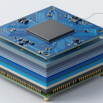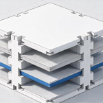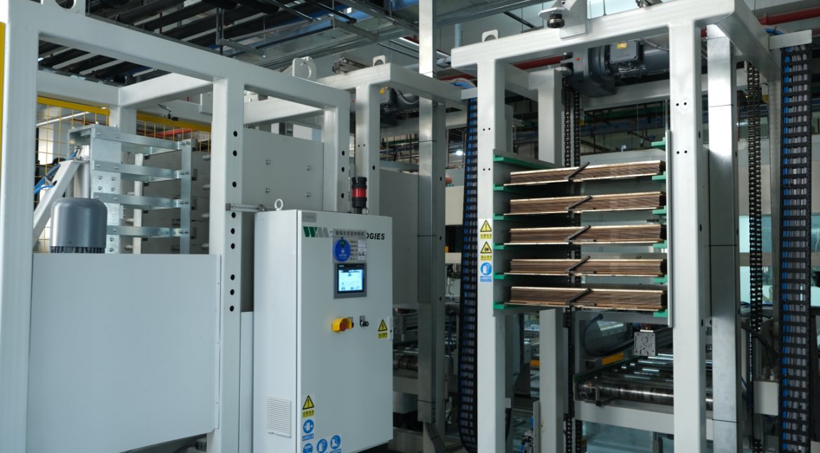
In high-volume multilayer PCB production, stacking multiple sheets of prepreg (PP) is a common method for achieving a specific dielectric thickness. When no single PP construction matches the target thickness, engineers may combine two or more sheets to build the required dielectric layer.
Although this approach can provide flexibility during stackup design, excessive PP stacking may increase material consumption, cutting waste, material handling, and lamination complexity.
A more production-oriented approach is to review the stackup from the beginning and determine whether the required dielectric thickness can be achieved with a standard single-sheet PP construction.
By combining stackup optimization, material availability, copper distribution, impedance requirements, and lamination capability, PCB manufacturers can reduce unnecessary PP combinations while maintaining electrical and mechanical performance.
Hidden Material Waste From Multiple PP Sheets
In conventional multilayer PCB design, engineers may select two or three thin PP sheets when the target dielectric thickness does not correspond to an available single-sheet specification.
For example, a design requiring approximately 0.20 mm of dielectric thickness might initially use two PP sheets with different nominal constructions.
This can create several types of hidden waste.
Cutting and Handling Waste
Every PP roll or sheet format has practical cutting limitations. Depending on the material width, panel dimensions, nesting strategy, and production setup, cutting can generate edge and end waste.
When a stackup requires several PP specifications, each additional material type may require separate:
- Material preparation
- Cutting operations
- Identification and storage
- Material transfer
- Production scheduling
- Inventory management
Therefore, reducing the number of PP types can improve material utilization and simplify production logistics.
Increased Process Complexity
Multiple PP sheets also create additional interfaces within the dielectric construction.
During PCB lamination, resin flows under heat and pressure to fill the spaces around inner-layer copper features and bond adjacent layers together. The final dielectric thickness depends on the PP construction, resin content, glass style, copper pattern, lamination conditions, and local geometry.
Adding more PP sheets does not automatically mean that the lamination process will become defective. However, a more complex material combination can make process control and material consistency more demanding.
For this reason, PP selection should be evaluated as part of the complete lamination process rather than solely by nominal thickness.
Prioritize Standard Single-Sheet PP Constructions
A practical principle for stackup optimization is to first review the manufacturer’s available PP library before finalizing the stackup.
Instead of defining an ideal dielectric thickness first and then trying to assemble it from multiple PP sheets, engineers can work backward from the available material portfolio.
A suitable workflow is:
- Review the manufacturer’s standard PP specifications.
- Determine the required final dielectric thickness.
- Establish the required impedance.
- Analyze inner-layer copper distribution.
- Compare available single-sheet PP constructions.
- Select candidate materials based on cured thickness and resin behavior.
- Validate the resulting stackup through simulation and process testing.
This approach helps prevent a common design problem: the PCB design is completed first, but the selected dielectric thickness cannot be produced efficiently with the manufacturer’s standard materials.
Nominal PP Thickness Is Not the Final Dielectric Thickness
One important consideration is that the nominal thickness of prepreg should not automatically be treated as the final dielectric thickness after lamination.
PP contains glass reinforcement and resin. During lamination, resin flows into the surrounding copper topography, while the overall dielectric thickness changes according to the material construction and process conditions.
The final thickness is influenced by:
- PP style
- Resin content
- Glass construction
- Copper thickness
- Copper coverage
- Copper distribution
- Lamination pressure
- Lamination temperature
- Heating and cooling profile
- Adjacent layer geometry
Therefore, a PP sheet with a nominal thickness slightly above or below the target does not necessarily produce the same final dielectric thickness.
For controlled-impedance designs, the cured dielectric geometry should be used in the impedance model rather than relying only on catalog nominal thickness.
Example of Replacing Multiple PP Sheets With One Construction
Consider an eight-layer PCB requiring approximately 0.20 mm of dielectric thickness between two copper layers.
An initial design might use two PP sheets to approximate the target thickness.
After reviewing the manufacturer’s material library, engineers may discover that a single PP construction can provide a similar cured dielectric thickness under the intended lamination conditions.
The revised stackup can then be evaluated for:
- Final dielectric thickness
- Resin flow
- Copper topography
- Impedance
- Lamination filling
- Board thickness
- Mechanical symmetry
- Material availability
If the single-sheet construction satisfies these requirements, it may reduce the number of PP materials involved in the stackup and simplify cutting and production handling.
The actual material-saving percentage should be calculated from the specific panel size, nesting efficiency, PP format, production volume, and material utilization rather than assuming a universal reduction.
When Multiple PP Sheets Are Necessary
Not every stackup can or should use a single PP sheet.
High-layer-count boards, unusual dielectric requirements, heavy copper structures, specialized materials, and controlled-impedance applications may require combinations of different PP constructions.
In such cases, the objective should not be to eliminate multiple PP layers at any cost. Instead, engineers should minimize unnecessary combinations while maintaining the required electrical and manufacturing performance.
Several strategies can help.
Reduce the Number of PP Types
When multiple sheets are necessary, using fewer PP specifications can simplify material management and cutting.
Where the final dielectric construction permits it, using repeated PP styles may be easier to control than combining many different materials.
However, different PP styles should not be replaced with a single material simply for convenience. The final cured thickness, resin content, glass style, impedance, and lamination behavior must remain within the required design window.
Improve Panelization and Cutting Efficiency
PP utilization is also affected by panel dimensions.
The PP cutting layout should be coordinated with the PCB panelization strategy so that the available material width is used efficiently.
A good cutting plan considers:
- Panel dimensions
- PP sheet or roll width
- Number of boards per panel
- Grain or material orientation where applicable
- Edge clearance
- Cutting kerf
- Manufacturing tolerances
Improving nesting efficiency can reduce edge waste without changing the electrical design.
Adjust the Target Dielectric Construction Carefully
In some cases, a small change in dielectric thickness may allow the use of a more standard PP combination.
However, such changes should only be made after reviewing impedance, creepage and clearance requirements, board thickness, mechanical constraints, and other design specifications.
A cost-driven stackup change should never compromise a controlled electrical requirement.
Consider Copper Distribution During PP Selection
PP selection should also be coordinated with the inner-layer copper pattern.
Large copper planes and dense copper regions create different lamination conditions from sparse routing areas. Resin must flow around the copper geometry to fill the required spaces and establish a reliable dielectric structure.
Therefore, PP layers should be evaluated together with:
- Inner-layer copper thickness
- Copper coverage
- Large copper areas
- Copper-free regions
- Via structures
- Local copper density
- Required dielectric thickness
This is particularly important for boards using heavy inner-layer copper.
A material construction that works well for a lightly populated signal layer may not behave identically between large copper planes.
Control Resin Flow When Reducing PP Combinations
Reducing the number of PP sheets changes the total resin and glass construction. This can influence resin flow during lamination.
If the selected PP construction does not provide sufficient resin to fill the relevant topography, potential issues may include:
- Resin starvation
- Voids
- Incomplete filling
- Poor interlayer bonding
- Local dielectric-thickness variation
- Delamination risk
Conversely, excessive resin flow can create other process-control challenges, including unwanted resin squeeze-out or changes in final dielectric thickness.
The correct solution is therefore not simply “use fewer PP sheets,” but rather to select a PP construction that provides an appropriate process window.
Recalculate Impedance After Stackup Changes
Any significant modification to the dielectric construction should trigger a new impedance calculation.
For controlled-impedance PCB designs, changes in dielectric thickness can directly affect the relationship between signal traces and their reference planes.
Important parameters include:
- Trace width
- Finished copper thickness
- Dielectric thickness
- Dielectric constant
- Reference-plane spacing
- Differential-pair spacing
- Trace geometry
- Manufacturing tolerances
After replacing multiple PP sheets with a single construction, the stackup model should therefore be updated.
For high-speed applications, impedance coupons and TDR measurements may be used to verify production results where required.
This ensures that material optimization does not unintentionally create electrical performance deviations.
Validate the Revised Lamination Structure
A revised stackup should be validated before being released for high-volume production.
A practical validation program may include:
Final Thickness Measurement
Measure the finished dielectric thickness at multiple locations to evaluate uniformity and confirm that the stackup remains within the specified tolerance.
Cross-Section Analysis
Microsection analysis can reveal:
- Voids
- Resin distribution
- Interlayer bonding
- Copper-to-resin interfaces
- Delamination
- Glass/resin structure
- Local dielectric thickness
Impedance Verification
For controlled-impedance boards, verify single-ended and differential impedance according to the project requirements.
Thermal Reliability Testing
Where appropriate, thermal stress or thermal cycling testing can be used to evaluate interlayer reliability.
For example, solder-float or other thermal-stress methods may be specified depending on the applicable qualification standard and customer requirements. The test temperature and duration should follow the relevant qualification procedure rather than being treated as a universal requirement.
Material Cost Should Not Be Evaluated in Isolation
The economic benefit of reducing PP sheets is not limited to the purchase price of the material.
A complete cost evaluation should consider:
Material cost + cutting waste + handling cost + inventory complexity + process yield + inspection cost + potential rework.
A single-sheet PP construction may reduce material handling and cutting complexity, but it must still maintain adequate lamination performance.
If a material reduction increases production defects, the apparent material savings can quickly be offset by scrap, rework, additional inspection, and production delays.
Therefore, the correct objective is to minimize total manufacturing cost rather than simply minimize PP quantity.
A Practical Stackup Optimization Workflow
A production-oriented multilayer PCB stackup workflow can follow these steps:
Step 1: Define Electrical Requirements
Establish target impedance, dielectric thickness, board thickness, layer count, copper thickness, and other electrical requirements.
Step 2: Review Available PP Materials
Obtain the manufacturer’s current PP material library, including available styles, resin contents, and expected cured thicknesses.
Step 3: Analyze Inner-Layer Copper
Review copper thickness and local copper distribution on every inner layer.
Step 4: Compare Single-Sheet Options
Determine whether a standard single-sheet PP can meet the required dielectric construction.
Step 5: Minimize Multiple-Sheet Combinations
If multiple sheets are unavoidable, minimize unnecessary PP types and optimize the combination for production stability.
Step 6: Review Panelization and Cutting
Coordinate PCB panel dimensions with PP cutting dimensions to improve material utilization.
Step 7: Recalculate the Stackup
Update the complete stackup, including final dielectric thickness, board thickness, copper balance, and mechanical symmetry.
Step 8: Recalculate Impedance
Update the impedance model using the revised dielectric construction and actual material properties.
Step 9: Validate Lamination
Perform pilot production, cross-section analysis, thickness measurements, and other appropriate process checks.
Step 10: Release the Optimized Stackup
After successful validation, document the approved PP construction and manufacturing parameters for production control.
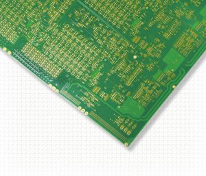
Kingda’s Multilayer PCB Stackup Optimization
Kingda provides engineering support for multilayer PCB stackup development and manufacturing optimization.
Our approach can consider PP material availability, copper distribution, copper thickness, dielectric requirements, impedance targets, lamination conditions, panelization, and production tolerances as an integrated system.
Rather than selecting multiple PP sheets simply because their nominal thicknesses add up to a target value, Kingda can evaluate whether a more standardized construction can achieve the required final dielectric thickness and manufacturing performance.
For applications where multiple PP sheets remain necessary, the stackup can also be optimized to reduce unnecessary material types, improve cutting utilization, and maintain stable lamination conditions.
Conclusion
Multiple PP sheets are sometimes necessary in multilayer PCB manufacturing, but they should not automatically be the default solution for achieving a target dielectric thickness.
By reviewing the manufacturer’s standard prepreg library before finalizing the stackup, engineers can identify opportunities to use single-sheet constructions where technically appropriate.
A comprehensive stackup optimization process should also consider copper distribution, resin flow, panelization, cutting efficiency, impedance, lamination reliability, and production tolerances.
The goal is not simply to reduce the number of PP layers. The goal is to establish a more efficient and repeatable manufacturing structure that reduces material waste while maintaining electrical performance and production quality.
With a systematic approach to PCB manufacturing, PP selection can become part of overall cost and process optimization rather than an isolated material-selection decision.