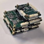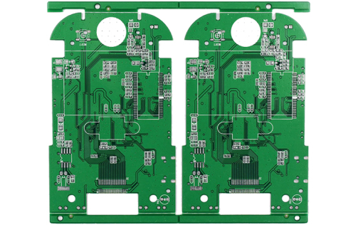
Medical electronics place higher demands on PCB performance than many conventional electronic products. In addition to electrical functionality, a Medical PCB must consider reliability, manufacturability, traceability, cleanliness, and long-term stability. These requirements become particularly important in patient monitoring and life-monitoring equipment, where unstable electrical performance can affect the accuracy of collected signals.
A typical 4-layer PCB for a portable medical monitoring module may contain fine traces, protective guard structures, precision differential routing, small pads, and dense component placement. If these characteristics are not reviewed during an early DFM review, a prototype may function normally while the same design develops defects during pilot or mass production.
Potential problems include inner-layer shorts or opens, registration-related defects, solder mask bubbles, insufficient annular rings, via reliability issues, and contamination-related insulation problems. For medical products, such defects can result in scrap, production delays, additional qualification work, and potentially significant project schedule impact.
Project Background and Hidden Manufacturing Risks
The project involved a portable hospital-use life-monitoring module using a 4-layer PCB. The initial prototypes passed functional testing, but during pilot production, a certain percentage of boards experienced inner-layer opens and hole-position deviations. Solder mask bubbles were also observed around areas containing protective guard structures.
Because the PCB was intended for medical equipment, simply repairing defective boards was not considered an appropriate solution for the production process. Defective units could require rejection and replacement, increasing material consumption and extending the manufacturing cycle.
The original design included several challenging characteristics:
- Approximately 0.12 mm fine traces
- Multiple small-diameter vias
- Analog signal areas with protective guard structures
- Approximately 1.0 mm finished board thickness
- Requirements for low ionic contamination
- High insulation resistance
- Precision analog and differential signal routing
- Dense component and pad distribution
The original manufacturing data was released without a dedicated medical-focused DFM review. Several design parameters were close to the manufacturer’s process limits. Although the prototype was functional, the design had limited process margin for stable volume production.
This illustrates an important principle: PCB manufacturing capability should not be evaluated only by whether a manufacturer can produce a single prototype. The more important question is whether the design can be manufactured consistently within the required quality and reliability window.
Key DFM Review Areas for a Medical 4-Layer PCB
Layer Registration and Inner-Layer Clearance
Laminate pressing can introduce dimensional changes and layer-to-layer registration variation. The effect becomes more significant when fine traces, small vias, and narrow clearances are combined in a multilayer design.
During the DFM review, designers and manufacturers should examine the relationship between:
- Via diameter and pad diameter
- Via-to-inner-copper clearance
- Trace-to-plane spacing
- Layer-to-layer registration
- Copper distribution
- Finished board thickness
- Material construction and lamination characteristics
A via positioned too close to an inner-layer copper area may have sufficient clearance in the CAD database but become vulnerable when manufacturing tolerances are considered.
Therefore, the design should not simply meet the nominal minimum value. A practical manufacturing margin should be established based on the PCB fabricator’s actual process capability.
For the project described here, several vias were initially positioned very close to internal copper areas. The spacing was increased during the DFM stage to provide additional process margin and reduce the risk of registration-related shorts.
Protective Guard Structures and Solder Mask
Protective guard rings or guard traces are commonly used around sensitive analog circuits to help control leakage and unwanted coupling. However, these structures can create manufacturing challenges when they form dense copper patterns with narrow gaps.
Large or closely spaced copper areas can affect solder mask application and curing. Depending on the geometry and process conditions, insufficient openings or narrow spaces may contribute to incomplete coating, trapped process residues, bubbles, or adhesion problems.
The DFM review should therefore evaluate both the electrical function and manufacturing characteristics of the guard structure.
Potential optimization measures include:
- Reviewing solder mask openings
- Increasing solder mask bridge where appropriate
- Avoiding unnecessarily narrow copper gaps
- Improving the spacing between adjacent copper features
- Reducing enclosed or difficult-to-process regions
- Checking solder mask expansion against actual fabrication capability
- Reviewing copper balance around sensitive areas
These changes should be verified against the electrical purpose of the guard structure. A manufacturing improvement should not unintentionally create a new leakage or coupling path.
Trace Width, Spacing, and Etching Margin
Fine-line routing is another important consideration for medical electronics.
The original design used approximately 0.12 mm traces for sensitive differential and analog signals. Such dimensions may be manufacturable under controlled conditions, but the available process margin depends on copper thickness, laminate construction, etching process, panel design, line density, and manufacturer capability.
A design that works during prototype production does not necessarily provide the same process window during larger-volume production.
During the DFM review, the engineering team evaluated whether the trace width could be increased from approximately 0.12 mm to 0.15 mm. The small increase in routing area had limited impact on the overall PCB layout while providing greater manufacturing margin.
The general design principle is to avoid unnecessarily pushing trace width and spacing toward the minimum fabrication capability when the electrical design does not require it.
For precision circuits, this is particularly useful because manufacturing variation can affect not only physical yield but also impedance, resistance, parasitic capacitance, and signal behavior.
Via Diameter and Annular Ring Verification
Small vias are often necessary when PCB space is limited. However, reducing via dimensions also reduces manufacturing margin.
The medical device PCB design review should examine:
- Finished hole diameter
- Drill diameter
- Pad diameter
- Annular ring
- Aspect ratio
- Hole-position tolerance
- Plating requirements
- Via-to-copper clearance
- Via-to-via spacing
A sufficiently robust annular ring helps accommodate drilling and registration variation. For designs using very small vias, the fabricator should confirm that the selected dimensions are appropriate for the actual production process rather than relying solely on nominal CAD values.
If the electrical design permits a slightly larger via or pad, the additional area may provide useful manufacturing margin with minimal impact on circuit performance.
Ionic Contamination and Insulation Reliability
Low ionic contamination is particularly important for high-impedance analog circuits and medical monitoring applications.
Residual ionic materials can contribute to surface leakage or electrochemical migration under suitable combinations of humidity, electrical bias, temperature, and contamination. In a high-impedance signal acquisition circuit, even relatively small leakage paths may affect measurement stability.
Therefore, PCB reliability should be considered together with manufacturing cleanliness.
During DFM, engineers should identify geometries that are difficult to clean, such as:
- Extremely narrow gaps
- Deep or enclosed copper structures
- Dense component regions
- Areas with restricted cleaning access
- Unnecessary copper cavities
- Structures that can trap process residues
Design optimization alone cannot guarantee cleanliness. Material selection, chemical process control, cleaning procedures, drying, handling, and cleanliness verification must also be controlled during manufacturing.
For critical medical products, ionic contamination testing and insulation-related verification should be defined according to the product’s applicable requirements rather than using a single universal acceptance value.
Why Prototype Success Does Not Guarantee Mass Production
One of the most common mistakes in PCB development is treating prototype functionality as proof of manufacturing readiness.
A prototype may pass because:
- Production volume is small
- Process operators can perform additional controls
- Individual boards receive more inspection
- Manufacturing variation has not accumulated across a larger production run
- The design happens to fall within the process window for that batch
Mass production introduces additional variables, including material variation, panel utilization, etching uniformity, drilling accuracy, lamination registration, solder mask processing, and equipment-to-equipment differences.
This is why PCB manufacturing readiness should be evaluated before the design is released for volume production.
An effective DFM process asks not only, “Can this PCB be manufactured?” but also, “Can it be manufactured repeatedly with sufficient process margin?”
DFM Optimization and Pilot Production
After the first manufacturing issues were identified, the design underwent a dedicated DFM optimization process.
The major changes included:
- Increasing critical trace width where electrical constraints allowed.
- Increasing clearance between vias and internal copper.
- Reviewing annular ring dimensions and hole-position tolerances.
- Optimizing protective guard structures.
- Improving solder mask spacing and openings.
- Reducing difficult-to-clean geometries.
- Reviewing the overall material stackup and manufacturing process.
- Adding targeted inspection and reliability verification.
After the changes, the second pilot run showed a substantial improvement in production yield, and the previously observed layer-registration and solder-mask-bubble issues were not observed in the same manner.
The result demonstrates the value of moving manufacturing analysis to the beginning of the product-development cycle rather than treating it as a final production inspection.
Actual yield improvements will vary according to the design, process capability, production volume, and inspection criteria, so individual project results should not be treated as universal manufacturing benchmarks.
Building DFM Into the Medical PCB Development Process
For a medical product, DFM review should ideally begin before prototype fabrication.
A practical workflow can include the following stages:
1. Design data review
Check Gerber or ODB++ data, drill files, stackup information, fabrication drawings, BOM, and assembly requirements for consistency.
2. Manufacturing capability comparison
Compare trace width, spacing, hole dimensions, annular rings, copper thickness, board thickness, and registration requirements against the selected fabricator’s actual process capability.
3. Medical reliability review
Identify high-impedance circuits, patient-monitoring interfaces, sensitive analog sections, power domains, isolation structures, and areas where contamination or moisture could affect electrical performance.
4. DFM optimization
Modify dimensions or structures that provide insufficient process margin while preserving electrical and mechanical requirements.
5. Prototype verification
Confirm that the revised design meets electrical, mechanical, and assembly requirements.
6. Pilot production
Evaluate manufacturing consistency under production-representative conditions rather than relying exclusively on prototype results.
7. Reliability and cleanliness verification
Depending on the product requirements, testing may include insulation resistance, ionic contamination, environmental exposure, thermal cycling, solderability, and other applicable qualification tests.
8. Production release
Only after the manufacturing and reliability requirements have been reviewed should the finalized design be released for volume production.
Kingda’s Approach to Medical PCB Manufacturing
For complex medical electronics, a capable PCB supplier should contribute more than basic fabrication. The manufacturer should be able to identify potential production risks during the engineering stage and communicate them before they become costly manufacturing problems.
Kingda can support medical PCB projects by combining design-for-manufacturing analysis with PCB fabrication and quality control. For applications involving fine traces, multilayer structures, sensitive analog circuits, small vias, controlled impedance, and high-reliability requirements, early communication between the PCB designer and manufacturer can help establish realistic manufacturing margins.
For medical monitoring applications, the DFM process can focus on:
- Fine-line and spacing capability
- Multilayer registration
- Small-hole manufacturing
- Copper distribution
- Solder mask processing
- Surface cleanliness
- Insulation reliability
- Material and stackup selection
- Manufacturing traceability
- Prototype-to-production consistency
The specific manufacturing and qualification requirements should always be determined according to the product design, applicable industry standards, regulatory requirements, and intended operating environment.
Conclusion
A successful medical PCB prototype is only one step toward reliable volume production. For sensitive Medical PCB designs, manufacturing risks can remain hidden until the production scale increases.
Early DFM review helps identify insufficient clearances, fine-line risks, small-hole limitations, solder mask challenges, contamination-sensitive structures, and other potential manufacturing defects before they become expensive production problems.
For a 4-layer PCB used in life-monitoring equipment, DFM should not focus only on whether the board can be fabricated. It should also consider process margin, electrical stability, cleanliness, long-term PCB reliability, and production consistency.
By involving the PCB manufacturer early, engineers can replace unnecessary process-limit designs with more robust structures, improve production readiness, reduce avoidable scrap and rework, and create a more controlled path from prototype development to medical device production.
Kingda can work with engineering teams from the early DFM stage to evaluate PCB manufacturability and help develop practical manufacturing solutions for medical and other high-reliability electronic applications.