When engineers evaluate cost-effective alternatives to premium high-frequency laminates, they often focus primarily on dielectric constant (Dk and Df) and dissipation factor (Dk and Df). While these parameters are essential for high-speed signal design, matching them alone does not guarantee equivalent electrical or manufacturing performance.
In real-world PCB development, differences in the glass-weave effect, moisture absorption, CTI, and copper foil roughness can affect impedance consistency, insertion loss, environmental stability, and long-term reliability. These parameters should therefore be evaluated together when selecting PCB material alternatives for high-speed applications.
A practical material replacement strategy should consider the complete signal path, including laminate structure, resin system, glass style, copper foil, stackup, routing, fabrication capability, and operating environment.
1. Glass-Weave Effect: An Often-Overlooked Challenge
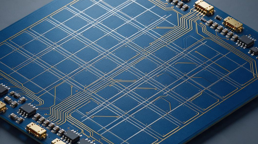
Glass fiber provides mechanical reinforcement in most FR-4 and low-loss laminate systems. The dielectric properties of glass fiber and resin are different, creating local variations in the effective dielectric environment around a transmission line.
When a high-speed differential pair runs in an unfavorable relationship with the glass-fiber weave, the two conductors may experience slightly different local dielectric conditions. This can create differential skew and contribute to signal integrity problems, particularly as data rates increase.
Premium high-frequency materials may use specialized glass styles, spread glass, or glass-free constructions to reduce this effect. However, many cost-effective FR-4-based high-speed PCB materials still rely on conventional glass fabrics.
The impact becomes more important as data rates, channel lengths, and timing margins become more demanding. Instead of assuming that a laminate with similar nominal Dk and Df will behave identically, engineers should consider glass style and routing orientation during material qualification.
For sensitive differential interfaces, practical mitigation methods may include:
- Using spread-glass or low-skew glass styles where available
- Reviewing the relationship between differential pairs and the glass-weave direction
- Using appropriate routing angles or trace positioning
- Evaluating skew and insertion loss through simulation and prototype testing
- Comparing actual impedance and eye-diagram performance rather than relying only on datasheet values
The glass-weave effect is therefore an important consideration when evaluating PCB material alternatives for high-speed links.
2. Moisture Absorption and Humidity Aging Affect Long-Term Performance
Moisture absorption is another parameter that is easily overlooked during material substitution.
When a PCB laminate absorbs moisture, the dielectric properties of the resin system can change. This may affect effective Dk, Df, impedance, and transmission loss. The magnitude of the change depends on the resin chemistry, glass structure, construction, environmental conditions, and measurement method.
For this reason, room-temperature datasheet values alone may not fully describe long-term behavior.
When evaluating high-speed PCB materials for outdoor, industrial, automotive, or other humid environments, engineers should review:
- Water absorption specifications
- Dk and Df stability under elevated humidity
- Insulation resistance after humidity exposure
- Dimensional stability
- Temperature and humidity cycling performance
- Changes in impedance or insertion loss after environmental conditioning
Rather than applying a single universal water-absorption threshold to every design, the appropriate limit should be determined according to the product’s operating environment and reliability requirements.
For demanding applications, accelerated environmental testing can provide more useful information than comparing initial datasheet values alone. This is particularly important when a low-cost laminate is being considered as one of the PCB material alternatives to a premium high-frequency material.
3. CTI: A Critical Parameter for Safety-Related Designs
Comparing only high-frequency electrical properties can create another problem: the replacement material may not meet the product’s insulation and safety requirements.
The Comparative Tracking Index (CTI) indicates the resistance of an insulating material to the formation of conductive tracking under specified test conditions. It can be particularly important for PCB assemblies that combine high-voltage and low-voltage circuits or operate in environments where contamination and humidity may increase insulation risks.
Applications such as industrial controls, power electronics, energy storage systems, and BMS designs may therefore require CTI to be considered alongside high-speed electrical performance.
A laminate can have suitable Dk and Df while still failing to meet the required CTI classification for a specific product or standard. Material substitution should therefore verify the applicable CTI requirement rather than assuming that all low-loss laminates provide equivalent insulation performance.
Another important consideration is the complete laminate construction. The core material and prepreg system should be evaluated together. Changing the core while retaining a different prepreg system can alter the electrical, mechanical, thermal, and insulation characteristics of the finished PCB.
Therefore, successful PCB material alternatives should be qualified at the stackup level rather than by evaluating the core material in isolation.
4. Copper Foil Roughness and Conductor Loss Must Be Evaluated Together
As signal frequency increases, conductor loss becomes increasingly important. The skin effect causes high-frequency current to become concentrated toward the conductor surfaces, making copper surface roughness an important factor in transmission-line loss.
This becomes particularly relevant when using low-loss laminates.
If a cost-effective laminate provides a lower Df but is paired with relatively rough copper foil, the reduction in dielectric loss may be partially offset by increased conductor loss. As a result, the overall channel improvement may be much smaller than expected.
For demanding high-speed designs, engineers can evaluate low-profile copper foil, such as LP or VLP copper, when supported by the laminate supplier and fabrication process.
However, copper foil selection should not be treated as an isolated material upgrade. The actual result depends on:
- Copper surface roughness
- Copper thickness
- Trace geometry
- Signal frequency
- Transmission-line structure
- Reference-plane configuration
- Etching process
- Manufacturing variation
When comparing PCB material alternatives, the laminate and copper foil should therefore be evaluated as a complete transmission-line system.
5. Dk and Df Are Essential—but They Are Not the Whole Story
Dk and Df remain fundamental parameters for high-speed PCB material selection, but they should not be used as the only criteria.
A more complete evaluation should consider:
| Parameter | Potential Impact |
|---|---|
| Dk and Df | Impedance, propagation delay, and dielectric loss |
| Glass-weave effect | Differential skew and local dielectric variation |
| Moisture absorption | Electrical stability and environmental reliability |
| CTI | Insulation and tracking resistance |
| Copper foil roughness | High-frequency conductor loss |
| Resin system | Thermal, mechanical, and electrical stability |
| Glass style | Dk uniformity and skew behavior |
| CTE | Dimensional stability and reliability |
| Thermal performance | Temperature-dependent electrical and mechanical behavior |
| Manufacturing compatibility | Yield, impedance consistency, and process stability |
This broader evaluation helps prevent a common substitution mistake: selecting a material that appears equivalent on paper but produces different results after PCB fabrication.
6. Validate the Material Through the Complete PCB Process
A datasheet comparison should be treated as the starting point rather than the final qualification step.
For a high-speed PCB material replacement project, engineers should consider a structured validation process:
Step 1: Define the electrical requirements
Identify the target impedance, data rate, channel length, insertion-loss budget, return-loss requirements, and allowable timing margin.
Step 2: Compare material properties
Evaluate Dk, Df, glass style, moisture absorption, CTI, CTE, copper foil options, and thermal properties.
Step 3: Review the stackup
Check dielectric thickness, copper thickness, reference planes, differential-pair geometry, and manufacturing tolerances.
Step 4: Perform simulation
Use field-solver or channel-simulation methods to evaluate impedance, propagation delay, insertion loss, return loss, and potential skew.
Step 5: Build representative prototypes
Prototype testing should use the actual laminate construction, copper foil, fabrication process, and representative routing structures.
Step 6: Verify environmental performance
Where required, evaluate temperature, humidity, thermal cycling, insulation performance, and other application-specific reliability conditions.
Step 7: Confirm mass-production consistency
Before approving the replacement for volume production, verify material traceability, laminate thickness, copper thickness, impedance consistency, surface quality, and process capability.
This approach reduces the risk of discovering material-related problems only after production tooling, certification, or system-level debugging has already begun.
7. A Cost-Effective Replacement Is a System-Level Optimization
The goal of replacing a premium high-frequency laminate is not simply to find a cheaper material with similar Dk and Df.
A successful replacement should provide an acceptable balance among:
- Electrical performance
- Signal integrity
- Environmental stability
- Safety requirements
- Thermal performance
- Manufacturing capability
- Production yield
- Material cost
- Long-term reliability
In some short-channel or moderately demanding applications, a carefully selected low-loss FR-4 system may provide a practical alternative to more expensive high-frequency materials. In more demanding applications, particularly those with long high-speed channels, tight loss budgets, severe environmental conditions, or RF/microwave requirements, a specialized laminate may still be necessary.
The correct decision should therefore be based on measured performance and application requirements rather than material price or nominal Dk/Df values alone.
Conclusion
When selecting high-speed PCB materials, engineers should look beyond Dk and Df. The glass-weave effect, moisture absorption, CTI, and copper foil roughness can all influence electrical performance, manufacturing stability, and long-term reliability.
A cost-effective material substitution should be validated through stackup design, simulation, prototype testing, environmental evaluation, and manufacturing qualification. By treating the laminate, copper foil, PCB structure, and fabrication process as one system, engineers can identify suitable PCB material alternatives while reducing the risk of impedance drift, signal-integrity degradation, and reliability problems.
Kingda can support high-speed PCB fabrication with impedance-controlled manufacturing and application-specific material evaluation, helping engineers move from material selection and prototype verification toward stable mass production.