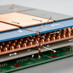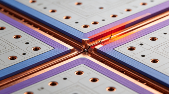
In high-density interconnect (HDI) PCB manufacturing, stackup misalignment is more than a cosmetic dimensional deviation. Even a small layer shift can affect microvia geometry, solder-joint reliability, impedance continuity, and thermal-mechanical stress distribution.
For example, when a customer reports an unexpected increase in BGA solder-joint failures after assembly, the root cause may not necessarily be the SMT process. If the HDI stackup shifts during lamination, uneven resin flow, copper distribution, thermal expansion, and mechanical constraints can interact and amplify the original alignment deviation.
The key engineering issue is therefore not simply the magnitude of the offset, but why the layers move, where the movement occurs, and whether the resulting geometry remains within the design and manufacturing tolerances.
What Causes HDI Stackup Misalignment During Lamination?
The fundamental cause of stackup misalignment is often the interaction between prepreg flow, copper pattern distribution, temperature, pressure, and material properties during lamination.
During a typical multilayer lamination cycle, prepreg softens as temperature increases and its viscosity changes significantly. At the same time, different copper pattern densities create different mechanical and thermal conditions across the panel.
Areas with large copper planes, such as power or ground regions, behave differently from areas with sparse signal routing. Uneven copper distribution can therefore produce nonuniform resin flow and local mechanical forces.
As the prepreg flows under pressure, adjacent copper layers can experience lateral movement. The actual amount of movement depends on several factors, including:
- Prepreg resin content and flow characteristics
- Copper pattern density and distribution
- Lamination temperature and pressure profile
- Heating and cooling rates
- Panel size and thickness
- Stackup symmetry
- Tooling and registration method
- Material CTE and mechanical properties
Therefore, it is not technically appropriate to assign one universal resin-viscosity value or one fixed time window to all FR-4 or HDI laminations. Each material system and lamination recipe must be evaluated using its own process data.
Why Does a Small Layer Shift Affect Reliability?
A small layer offset can become more significant when it occurs around microvias, fine-pitch BGA structures, or other high-density features.
Consider a microvia designed at the center of a target pad. If the layer registration shifts during lamination, subsequent laser drilling may leave the actual via position closer to the pad edge than intended.
This reduces the available copper margin around the microvia and may increase the sensitivity of the structure to plating variation, thermal cycling, and mechanical stress.
The relationship can be summarized as:
Stackup misalignment → target-pad displacement → reduced microvia margin → higher local stress concentration → increased reliability risk
This does not mean that every small offset will cause failure. Reliability depends on the complete via structure, pad dimensions, copper thickness, dielectric construction, plating quality, thermal history, and application environment.
Three Reliability Risks Associated With HDI Misalignment
1. Microvia Reliability Can Be Reduced
Microvia structures are particularly sensitive to registration accuracy because their geometrical margins are relatively small.
When a microvia moves toward the edge of its target pad, the remaining annular copper area becomes smaller. Variations in laser drilling, desmear, electroless copper, and electrolytic plating can then have a greater effect on the final structure.
During thermal cycling, the mismatch in expansion between copper, resin, and surrounding materials generates repeated mechanical stress.
Potential failure modes include:
- Microvia barrel cracking
- Interface separation
- Pad cratering
- Interconnection defects
- Copper fatigue
- Crack propagation around the target pad
The appropriate acceptance criteria should be determined according to the PCB class, design geometry, applicable standards, and qualification requirements rather than using one fixed offset value for every HDI design.
2. Signal Integrity Can Be Affected
HDI stackup accuracy also matters for high-speed signal transmission.
A layer shift can change the relative position between a signal trace and its reference plane. This may alter the effective dielectric geometry and therefore affect characteristic impedance, coupling, and return-current distribution.
The impact becomes more important when the design contains:
- High-speed differential pairs
- Fine-pitch escape routing
- Controlled-impedance traces
- Narrow dielectric spacing
- High-density via fields
- Long high-speed channels
Instead of assuming that a specific layer shift will always produce a fixed eye-height reduction or crosstalk increase, engineers should evaluate the actual stackup using field-solver analysis, impedance calculations, and signal-integrity simulation.
For high-speed HDI designs, the goal is not simply to minimize the absolute offset. It is to keep the actual dielectric thickness, reference-plane relationship, trace geometry, and via transitions within the electrical tolerance required by the design.
3. Thermal-Mechanical Stress Can Become Concentrated
FR-4 and copper have significantly different coefficients of thermal expansion. Copper has a relatively low CTE, while the resin system exhibits substantially greater expansion, particularly in the Z-axis.
During heating and cooling, this difference produces mechanical stress within multilayer structures.
When PCB CTE mismatch interacts with a geometrically shifted microvia or pad, the stress distribution may become asymmetric. A local structure can therefore experience higher stress than a geometrically centered structure.
This is especially important for:
- High-layer-count HDI boards
- Stacked microvias
- Large BGA packages
- Thin-core constructions
- Large copper-plane structures
- Applications exposed to repeated temperature changes
Finite-element analysis can help identify local stress concentrations, but simulation results should be correlated with cross-section analysis and reliability testing before being treated as production evidence.
How Stackup Design Influences Layer Movement
One of the most overlooked factors in HDI stackup design is copper balance.
A large copper plane on one layer combined with sparse routing on another layer can create significant differences in resin-flow behavior during lamination.
For example, if a power layer contains extensive copper while the adjacent signal layer contains mostly narrow traces and open areas, the resin may flow differently across the panel. This can contribute to local layer movement.
A better approach is to evaluate copper distribution during the PCB design stage.
Design teams should consider:
- Copper density by layer
- Copper balance across the panel
- Symmetry of the stackup
- Large-area copper distribution
- Resin thickness
- Prepreg selection
- Microvia arrangement
- BGA escape density
Copper balancing does not mean adding unnecessary copper everywhere. Uncontrolled copper addition can introduce other problems such as parasitic capacitance, thermal effects, manufacturing constraints, and unwanted coupling.
The objective is to achieve a manufacturable and mechanically balanced structure while maintaining the required electrical performance.
Material Selection: Prepreg Flow Matters
Prepreg selection has a direct influence on lamination behavior.
Instead of simply choosing a material based on nominal flow percentage, engineers should evaluate the complete material datasheet and actual production behavior, including:
- Resin content
- Flow characteristics
- Glass style
- Cure behavior
- Tg
- Z-axis CTE
- Thickness after lamination
- Thermal expansion behavior
- Lamination pressure requirements
A lower-flow prepreg can help control excessive resin movement in certain HDI constructions, but it is not automatically the best choice.
If resin flow is insufficient, engineers may encounter incomplete filling, voids, poor bonding, or inadequate coverage around dense copper features.
Therefore, prepreg selection should be coordinated with stackup thickness, copper distribution, via structure, and the manufacturer’s lamination process window.
Design Guidelines for Microvia and BGA Structures
When working with fine-pitch HDI structures, designers should reserve sufficient geometric margin around microvias and BGA pads.
Important parameters include:
- Microvia diameter
- Capture-pad diameter
- Land diameter
- Annular ring
- Pad-to-pad spacing
- Laser-drilling tolerance
- Layer-to-layer registration tolerance
- Plating thickness
- BGA pitch
A larger pad may provide greater tolerance to registration variation, but it can also reduce routing density.
Consequently, there is no single universal pad diameter or annular-ring value that guarantees reliability. The appropriate dimensions should be established by combining electrical requirements, fabrication capability, IPC requirements, and reliability targets.
For critical HDI products, the design team should obtain the manufacturer’s actual registration capability before finalizing the layout.
Manufacturing Control: Measure Before Assembly
Post-lamination inspection is an important part of HDI manufacturing quality control.
Depending on the board structure and available equipment, manufacturers may use:
- X-ray inspection
- AOI
- Optical registration measurement
- Cross-section analysis
- Coupon verification
- Dimensional inspection
The purpose is not merely to determine whether a board exceeds an arbitrary offset limit. The measurement should verify whether the actual stackup remains compatible with the microvia, BGA, impedance, and mechanical design requirements.
For critical products, the process should establish a statistical baseline for layer registration rather than relying on one isolated measurement.
Key process data can include:
- Actual prepreg flow characteristics
- Lamination temperature and pressure profile
- Heating and cooling rates
- Layer-to-layer registration distribution
- Copper pattern density
- Post-lamination thickness
- Microvia registration results
This data can then be used for process capability analysis and continuous improvement.
Thermal Cycling and BGA Reliability
BGA solder joint reliability is affected by multiple variables, and HDI layer alignment is only one potential contributor.
Other important factors include:
- Package size
- BGA pitch
- PCB thickness
- Board stiffness
- Solder alloy
- Pad design
- Surface finish
- Temperature range
- Dwell time
- Number of cycles
- Assembly profile
- Component and PCB CTE
- Mechanical constraints
A BGA solder-joint crack observed after thermal cycling should therefore be investigated through a structured failure-analysis process.
Recommended analysis methods include:
- X-ray inspection
- Cross-sectioning
- Dye-and-pry analysis where appropriate
- Metallographic examination
- Solder-joint fracture analysis
- PCB registration measurement
- Warpage measurement
- Thermal-profile verification
This approach helps determine whether the primary cause is PCB deformation, solder fatigue, pad design, component warpage, assembly conditions, or HDI structural variation.
Common Engineering Mistake: Treating Misalignment as Only a Manufacturing Problem
A common mistake is to send a finished layout to the PCB manufacturer and expect the fabrication process to compensate for all geometric sensitivity.
In reality, PCB manufacturing reliability begins during design.
If a design contains extremely tight microvia margins, highly unbalanced copper distribution, aggressive dielectric tolerances, and large BGA packages simultaneously, even a manufacturing process operating within its normal capability range may produce a higher reliability risk.
A better DFM process should therefore review:
- Stackup symmetry
- Copper balance
- Microvia geometry
- BGA escape routing
- Registration tolerance
- Prepreg construction
- Impedance requirements
- Thermal expansion
- Panelization
- Lamination capability
The PCB manufacturer should be involved before the stackup is frozen, especially for high-layer-count HDI and fine-pitch BGA designs.
A Practical Three-Point Review for HDI Projects
Before releasing a critical HDI design for production, engineers can ask the PCB manufacturer for three categories of data.
1. Material data
Confirm the actual prepreg construction, resin characteristics, Tg, and CTE information used for the selected stackup.
2. Lamination data
Review the actual lamination temperature, pressure, heating profile, cooling profile, and process window.
3. Registration data
Review the measured layer-to-layer registration distribution from production panels or qualification coupons.
These three categories provide much more useful information than relying on a single nominal offset value.

Boundary Conditions and Engineering Validation
The mechanisms discussed above are particularly relevant to conventional FR-4-based HDI structures, but the actual behavior can vary substantially with different material systems.
High-frequency laminates, low-loss materials, high-Tg systems, hybrid constructions, and specialized resin systems may exhibit different flow, CTE, dielectric, and mechanical behavior.
Therefore, engineers should not assume that changing to a particular laminate will automatically eliminate the reliability risk.
For advanced designs, validation should combine:
- Material characterization
- Lamination trials
- Registration measurement
- Cross-section inspection
- Impedance verification
- Thermal cycling
- BGA reliability testing
- Failure analysis
How Kingda Can Support HDI Reliability Control
At Kingda, HDI reliability should be managed as a system-level engineering issue rather than as a single dimensional specification.
By coordinating material selection, stackup design, copper balancing, lamination parameters, registration control, microvia fabrication, and reliability validation, engineers can identify potential risks before they reach assembly and field operation.
The key principle is simple: HDI stackup misalignment should be controlled from design through lamination and verified before assembly—not treated as a problem only after BGA solder joints fail.
For demanding HDI applications, early DFM review and process validation can reduce the risk of registration-related defects while maintaining the electrical, mechanical, and reliability requirements of the finished PCB.