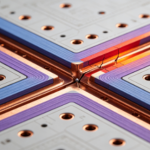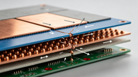
BGA solder joint failures can sometimes occur even when X-ray inspection shows no obvious defect and the soldering process appears to be well controlled. After repeated thermal cycling, cracks may develop at the solder-to-pad or solder-to-package interface, eventually causing intermittent electrical failures or open circuits.
One important cause is CTE mismatch between the semiconductor package, solder joints, PCB, and surrounding materials.
The coefficient of thermal expansion (CTE) describes how much a material expands or contracts as temperature changes. When two mechanically connected materials have significantly different CTE values, thermal cycling can repeatedly generate mechanical strain at their interface.
For BGA assemblies, this effect becomes more important as package size, PCB size, temperature range, and the number of thermal cycles increase. Therefore, PCB CTE and package construction should be considered during the early design stage rather than only after a reliability failure occurs.
1. How CTE Mismatch Drives Solder Joint Fatigue
Silicon has a relatively low CTE, typically around 2.6 ppm/°C, while organic PCB materials generally exhibit substantially different expansion behavior.
More importantly, a PCB does not have one single CTE value in every direction. The X/Y-plane CTE and Z-axis CTE can be significantly different.
For many FR-4 constructions, the in-plane CTE is relatively low because the glass reinforcement constrains expansion. Above the resin system’s glass-transition temperature, however, the resin can expand much more strongly, resulting in a substantially higher Z-axis CTE.
During temperature cycling, the PCB and package therefore do not expand and contract identically.
The resulting mechanical strain can be transferred through the BGA solder joints. Repeated temperature changes can produce cyclic shear and tensile stresses, and accumulated plastic deformation may eventually initiate fatigue cracks.
The simplified relationship can be expressed conceptually as:
[\Delta L = L \times \Delta CTE \times \Delta T]
where:
- (\Delta L) is the relative dimensional change
- (L) is the relevant mechanical dimension
- (\Delta CTE) is the difference in thermal expansion coefficients
- (\Delta T) is the temperature change
The actual solder-joint stress is more complicated because package structure, solder alloy, joint geometry, PCB stiffness, underfill, temperature-dependent material properties, and assembly constraints all contribute to the final mechanical response.
2. Z-Axis CTE Should Not Be Confused With X/Y CTE
One of the most common mistakes in PCB reliability analysis is using a laminate’s nominal X/Y CTE value as if it represented all three dimensions.
This is particularly problematic when evaluating BGA reliability.
Z-axis CTE describes expansion through the thickness of the PCB. It is strongly influenced by:
- Resin chemistry
- Resin content
- Glass style
- Laminate construction
- Glass-transition temperature
- Pressing conditions
- Copper distribution
- Temperature range
The Z-axis behavior can therefore differ significantly from the X/Y value listed on a conventional material datasheet.
For BGA applications with demanding thermal-cycling requirements, engineers should obtain the appropriate Z-axis CTE data using the relevant test method and temperature range.
Instead of relying on a generic FR-4 CTE value, the actual laminate construction should be evaluated.
3. Why Thermal Cycling Accelerates Solder Joint Fatigue
Thermal cycling repeatedly exposes the assembly to high and low temperatures. Each cycle produces differential expansion and contraction between the package, PCB, solder, and other structural materials.
Solder is not a perfectly elastic material. Under repeated mechanical loading and elevated temperature, it can undergo creep, plastic deformation, and fatigue damage.
Over many cycles, these mechanisms can interact and produce crack initiation and propagation.
The risk is influenced by:
- Temperature range
- Dwell time
- Ramp rate
- Number of cycles
- BGA package size
- Ball pitch
- Solder alloy
- PCB thickness
- PCB stiffness
- Component-to-board CTE mismatch
- Board-level constraints
Therefore, there is no single universal CTE-difference threshold that can accurately predict solder-joint lifetime for every BGA assembly.
A CTE mismatch value should be treated as an input to reliability analysis rather than as a stand-alone pass/fail criterion.
4. Package Size Makes the Problem More Significant
Larger BGA packages generally experience greater absolute displacement between the package and PCB when their thermal expansion behaviors differ.
This can increase the mechanical strain imposed on solder joints, particularly those located farther from the package neutral point.
Package size, ball pitch, substrate construction, solder alloy, and board stiffness should therefore be considered together.
For large BGA packages, engineers can use finite-element analysis to evaluate:
- Package deformation
- PCB deformation
- Solder-joint strain
- Stress distribution
- Critical solder-joint locations
- Fatigue-life trends
This approach provides more useful information than applying a single CTE limit to the entire PCB.
5. Where Do Cracks Usually Initiate?
When a BGA assembly fails after thermal cycling, the crack location provides important clues about the failure mechanism.
Potential failure locations include:
- Solder-to-PCB pad interface
- Solder-to-package interface
- Solder bulk
- Intermetallic compound (IMC) region
- PCB pad or copper interface
- PCB laminate
- Package substrate
A solder-joint crack can be difficult to identify with conventional X-ray inspection during the early stages because small fatigue cracks may not produce an obvious radiographic signature.
Cross-sectioning, dye-and-pry analysis where appropriate, metallographic inspection, electrical continuity monitoring, and other failure-analysis methods can provide additional evidence.
It is therefore not technically appropriate to conclude that every BGA crack originates at the PCB-side pad simply from the presence of a CTE mismatch. The actual fracture location must be verified through failure analysis.
6. PCB Material Selection Matters
Material selection is an important part of PCB reliability.
When a PCB is designed for wide temperature excursions, engineers should evaluate:
- X/Y CTE
- Z-axis CTE
- Tg
- Td
- Elastic modulus
- Moisture absorption
- Laminate thickness
- Glass construction
- Resin content
- Copper distribution
A high-Tg laminate can provide better dimensional and thermal stability in some applications, but high Tg alone does not guarantee long BGA solder-joint life.
The complete mechanical system must be considered.
For demanding applications, low-Z-CTE materials or specialized laminate constructions may reduce the thermal expansion difference between the PCB and package. However, their electrical, thermal, mechanical, and manufacturing properties must also be compatible with the overall design.
7. Solder Alloy and Surface Finish Are Secondary but Important Factors
CTE mismatch is only one part of solder joint reliability.
Solder alloy properties also influence fatigue behavior. Common lead-free alloys such as SAC-family solders exhibit temperature-dependent mechanical properties, and their creep and fatigue behavior must be considered under the actual thermal profile.
PCB surface finish can also influence solderability, intermetallic formation, pad structure, and interface reliability.
ENIG and ENEPIG should therefore be selected based on the complete assembly requirements rather than assuming that one surface finish is universally more reliable for BGA applications.
Surface finish selection should consider:
- Solderability
- Pad geometry
- Nickel and palladium structure
- IMC formation
- Assembly process
- Environmental requirements
- Required reliability level
If a failure investigation identifies an interface-related crack, the surface finish and metallurgical structure should be examined together with the CTE-related mechanical loading.
8. Avoid Using a Single CTE Number as a Pass/Fail Rule
A common engineering shortcut is to specify a single requirement such as:
“PCB Z-axis CTE must be below XX ppm/°C.”
A numerical requirement can be useful in a purchasing or engineering specification, but the correct value should come from the application’s reliability target and qualification methodology.
The required PCB CTE depends on:
- BGA package dimensions
- Package substrate CTE
- PCB construction
- Solder alloy
- Temperature range
- Number of thermal cycles
- Board thickness
- Component placement
- Mechanical constraints
- Expected service life
For this reason, a value that works for a small consumer BGA may not be appropriate for a large processor package or automotive control module.
9. Practical BGA Reliability Validation
A robust BGA solder joint fatigue evaluation should combine material characterization, simulation, prototype testing, and failure analysis.
Step 1: Define the Operating Environment
Determine the actual temperature range, thermal ramp rate, dwell time, expected cycle count, and service conditions.
Step 2: Characterize the PCB Material
Obtain X/Y and Z-axis CTE data over the relevant temperature range. Also review Tg, moisture behavior, modulus, and laminate construction.
Step 3: Review the BGA Package
Evaluate package size, substrate construction, ball pitch, solder alloy, and package CTE.
Step 4: Perform Mechanical Simulation
For large or high-reliability BGAs, finite-element analysis can help identify solder joints experiencing the highest cyclic strain.
Step 5: Build Representative Prototypes
Use the intended PCB stackup, surface finish, solder paste, BGA component, and assembly process.
Step 6: Conduct Thermal Cycling
Perform thermal cycling according to the applicable product qualification standard and operating requirements.
Step 7: Monitor Electrical Performance
Continuity monitoring during cycling can identify intermittent failures before they become permanent opens.
Step 8: Perform Failure Analysis
Use cross-sections and metallographic analysis to determine the actual crack location and distinguish solder fatigue from pad, IMC, laminate, or assembly-related failures.
10. How to Reduce CTE-Related BGA Risk
Several design approaches can reduce the risk associated with CTE mismatch:
- Select PCB materials with suitable thermal expansion characteristics
- Evaluate Z-axis expansion separately from X/Y expansion
- Optimize BGA pad and solder-joint geometry
- Avoid unnecessary PCB mechanical constraints around large BGAs
- Review board thickness and stiffness
- Optimize component placement
- Evaluate package and solder alloy compatibility
- Control moisture before assembly
- Validate the complete assembly through thermal cycling
- Use failure analysis to feed results back into material and layout selection
For large packages, additional structural measures such as underfill or other mechanical reinforcement may be considered when permitted by the assembly architecture. These solutions should be evaluated carefully because they can also change stress distribution elsewhere in the package.

11. The Key Point: CTE Mismatch Is a System-Level Reliability Issue
BGA failure cannot normally be attributed to one material parameter without evidence.
CTE mismatch can create cyclic mechanical strain, but the resulting BGA solder joint fatigue behavior is determined by the interaction of the PCB, package, solder, surface finish, assembly process, mechanical constraints, and thermal environment.
The most important distinction is between X/Y CTE and Z-axis CTE. Engineers should not substitute one for the other when evaluating PCB reliability.
For demanding products, material datasheets should be combined with package data, mechanical simulation, representative prototypes, and thermal cycling results.
Conclusion
The reliability of a BGA assembly depends on much more than solder paste and reflow-profile control. PCB CTE, package expansion, solder properties, board stiffness, and thermal cycling can interact to produce fatigue damage over time.
When evaluating BGA solder joint fatigue, engineers should pay particular attention to Z-axis CTE, package size, temperature range, and the complete PCB stackup. Rather than relying on a universal CTE threshold, the most reliable approach is to establish application-specific requirements and verify them through simulation and physical testing.
Kingda can support BGA PCB fabrication, controlled laminate selection, impedance-controlled manufacturing, and prototype reliability verification, helping engineers evaluate PCB material and construction choices before volume production.