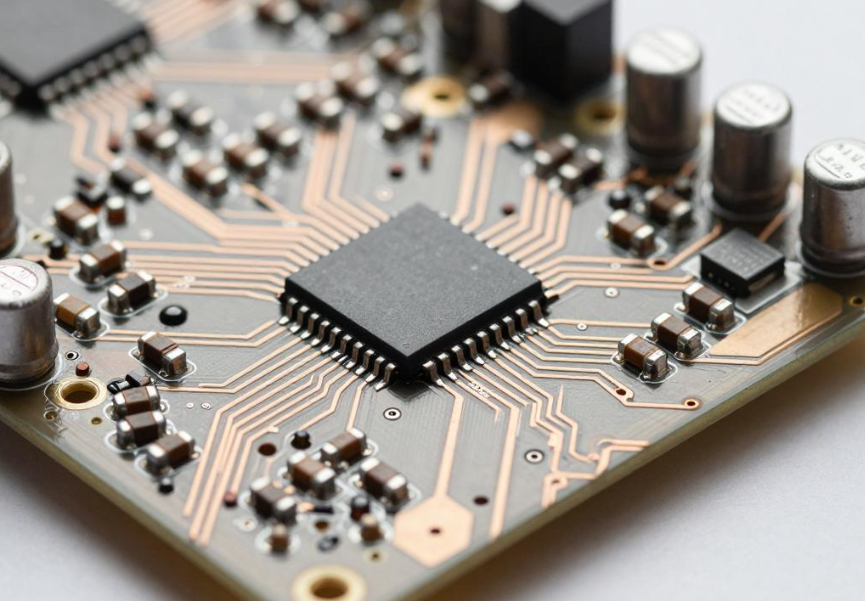
In RF communication, high-speed data acquisition, industrial Ethernet, and other demanding electronic applications, engineers often face a difficult material-selection problem. Traditional high-frequency laminates such as PTFE-based materials and hydrocarbon resin systems can provide excellent electrical performance, but their material costs, fabrication requirements, and supply conditions may increase the overall PCB cost.
For products moving from prototype development to mass production, material cost becomes an increasingly important part of the total BOM. However, assuming that every high-speed design requires a premium high-frequency laminate can result in unnecessary material and manufacturing expenses.
The development of cost-effective high-speed PCB materials provides additional options. Depending on channel length, operating frequency, loss requirements, stackup, environmental conditions, and fabrication capability, selected low-loss FR-4-based materials or modified resin systems may serve as practical PCB material alternatives.
The key is not simply to find a cheaper laminate with similar Dk and Df values. Engineers should evaluate the complete transmission channel, material properties, PCB construction, fabrication process, and reliability requirements before approving a substitution.
1. Why High-Frequency Materials Can Increase PCB Costs
PTFE-based laminates are widely used in demanding RF and microwave applications because of their low dielectric loss and useful high-frequency characteristics. However, some PTFE constructions can be more difficult to fabricate than conventional FR-4 materials.
Material cost is only one part of the equation. Drilling behavior, dimensional stability, copper adhesion, lamination conditions, plating compatibility, and process yield can also affect the final PCB price.
For multilayer designs, specialized materials may require tighter process control during lamination and registration. If a material has a narrow process window or requires special fabrication procedures, the manufacturing cost can increase even when the PCB layer count and dimensions remain unchanged.
Hydrocarbon-based high-frequency laminates can provide a balance between electrical performance and manufacturability, but they are generally more expensive than conventional FR-4. Their suitability should therefore be evaluated against the actual electrical requirements rather than selected solely because a design is classified as “high speed.”
A common misconception is that a data rate above a particular threshold automatically requires a premium RF laminate. In practice, material selection depends on the complete channel loss budget. Data rate is important, but it is only one of several factors.
For example, a relatively short high-speed channel with sufficient transmitter and receiver equalization may tolerate a higher-loss laminate than a much longer channel operating at the same data rate.
2. Cost-Effective High-Speed PCB Material Options
Modern high-speed PCB materials cover a wide range of electrical and manufacturing characteristics. For many digital applications, modified FR-4 systems can provide a useful balance between signal performance and cost.
Low-Loss FR-4
Low-loss FR-4 materials typically use modified resin systems to reduce dielectric loss compared with conventional FR-4. Their manufacturing processes can remain relatively close to standard FR-4 production, which can simplify drilling, lamination, plating, and other fabrication operations.
Depending on the specific grade, stackup, channel length, operating frequency, and loss budget, low-loss FR-4 may be suitable for a range of high-speed digital interfaces.
The actual Dk and Df values should always be taken from the material manufacturer’s specifications and evaluated using the appropriate test method and frequency.
Ultra-Low-Loss FR-4
Ultra-low-loss FR-4 materials further reduce dielectric loss and can be considered when a conventional low-loss FR-4 system does not provide sufficient channel margin.
These materials can be useful for longer differential channels, higher-speed interfaces, and applications where insertion-loss requirements are more demanding. In some cases, they may provide a practical alternative to more expensive high-frequency laminates.
However, material substitution should never be based on Df alone. Copper roughness, glass-weave effects, dielectric thickness, via transitions, connectors, and manufacturing tolerances can all contribute to total channel loss.
Modified PPO and Other Resin Systems
Modified PPO-based materials and other engineered resin systems can provide another category of PCB material alternatives. By combining different resin technologies, manufacturers can balance dielectric performance, thermal characteristics, mechanical properties, and manufacturing behavior.
These materials may be appropriate for communication equipment, high-speed backplanes, industrial networking, and other applications requiring improved electrical performance without necessarily using a premium PTFE construction.
Because resin systems and fabrication requirements vary between material grades, production trials should be completed before mass production approval.
3. Evaluate the Complete Signal Loss Budget
The signal loss budget should be one of the first considerations when evaluating a material replacement.
Instead of starting with the question, “Which material can support this data rate?” engineers should ask:
How much loss can the complete channel tolerate, and how much of that loss comes from the PCB?
A high-speed channel may contain several loss contributors:
- PCB dielectric loss
- Copper conductor loss
- Copper surface roughness
- Via transitions
- Connectors
- Package structures
- Trace discontinuities
- Reflections caused by impedance variation
The PCB laminate is therefore only one component of the overall channel.
For a short PCB trace, the accumulated dielectric loss may be relatively limited, making a cost-effective laminate a viable option. As the trace becomes longer or the operating frequency increases, dielectric and conductor losses can consume more of the available margin.
Engineers should calculate or simulate the signal loss budget before deciding whether a premium material is actually necessary.
4. Dk Stability Is More Important Than a Single Datasheet Number
Dielectric constant affects transmission-line impedance and propagation characteristics. However, the nominal Dk printed on a datasheet does not always represent the effective Dk of the final PCB transmission line.
The actual result can be influenced by:
- Measurement frequency
- Resin content
- Glass style
- Dielectric thickness
- Copper geometry
- Glass-weave distribution
- Temperature
- Moisture
- Manufacturing variation
Therefore, Dk stability should be evaluated together with the target operating frequency and actual PCB construction.
For high-speed differential pairs, variations in the local dielectric environment can also affect skew and signal integrity. This is particularly relevant when the differential pair interacts unfavorably with the glass weave.
When comparing PCB material alternatives, engineers should request material data at relevant frequencies and, where necessary, validate the effective electrical properties through test coupons or representative prototypes.
5. Manufacturing Compatibility Directly Affects Material Cost
Electrical performance is only half of the material-selection process. Manufacturing compatibility can determine whether a theoretically suitable material can actually be produced consistently and economically.
A material may appear attractive in simulation but become less economical if it requires:
- Special drilling parameters
- Different desmear conditions
- Tighter lamination control
- Special copper treatment
- Additional process steps
- Lower production yield
- Dedicated fabrication equipment
By contrast, some modified FR-4 systems can be processed using equipment and process flows already established for conventional multilayer PCBs.
This can reduce engineering complexity and improve production consistency.
When evaluating PCB material alternatives, engineers should therefore compare not only laminate prices but also total manufacturing requirements, expected yield, process capability, and production volume.
6. Copper Foil and Material Selection Should Be Evaluated Together
Low-loss dielectric material does not automatically guarantee low overall transmission loss.
At higher frequencies, conductor loss becomes increasingly important. The skin effect causes current to become concentrated toward the conductor surface, making copper surface roughness an important factor in high-speed transmission.
For demanding applications, low-profile or very-low-profile copper foil may help reduce conductor loss. However, the appropriate copper foil depends on the material construction, fabrication process, frequency, trace geometry, and reliability requirements.
A useful material evaluation should therefore consider:
- Dk and Df
- Copper roughness
- Copper thickness
- Glass style
- Dielectric thickness
- Trace geometry
- Surface finish
- Via structure
This system-level approach prevents engineers from improving one material parameter while unintentionally introducing another source of channel loss.
7. Define the Application Boundary Before Selecting a Replacement
Cost-effective high-speed PCB materials are not universal substitutes for premium RF or microwave laminates.
For short digital channels, moderate-loss applications, and designs with sufficient equalization and system margin, low-loss FR-4 or ultra-low-loss FR-4 may provide a practical balance between electrical performance and cost.
However, specialized materials may remain necessary for applications involving:
- Very long high-speed channels
- Extremely tight insertion-loss budgets
- High-frequency RF or microwave transmission
- Millimeter-wave applications
- Severe temperature or humidity conditions
- Strict dimensional stability requirements
- Specialized antenna structures
- High-performance RF impedance control
For these applications, a lower-cost laminate should only be approved after electrical and environmental validation.
The boundary should be determined by the actual design requirements rather than by a single data-rate threshold.
8. Prototype Validation Before Mass Production
Before replacing an established high-frequency laminate, engineers should complete a structured validation process.
Step 1: Define electrical requirements
Determine target impedance, operating frequency, data rate, channel length, insertion-loss limit, return-loss requirement, and available system margin.
Step 2: Establish the signal loss budget
Separate PCB dielectric loss, conductor loss, via loss, connector loss, and other channel contributions.
Step 3: Compare material properties
Review Dk, Df, glass style, copper foil roughness, moisture absorption, thermal characteristics, CTE, and other application-specific parameters.
Step 4: Review manufacturing compatibility
Confirm drilling, lamination, plating, solder mask, surface finish, and other fabrication processes.
Step 5: Build representative test coupons
Use the proposed material, copper foil, dielectric construction, and fabrication process to measure impedance and transmission performance.
Step 6: Perform system-level testing
Evaluate eye diagrams, insertion loss, return loss, BER where applicable, thermal performance, and environmental stability.
Step 7: Conduct production verification
Before volume production, verify material consistency, impedance capability, dimensional stability, process yield, and traceability.
This process allows engineers to determine whether a lower-cost material can meet the actual system requirements rather than relying exclusively on theoretical datasheet comparisons.
9. Cost Reduction Should Not Compromise Signal Integrity
The purpose of material substitution is not simply to reduce laminate price. A successful cost-reduction strategy should balance electrical performance, manufacturing efficiency, reliability, and total product cost.
For suitable applications, modified FR-4-based materials can reduce material and fabrication costs while providing adequate high-speed performance. In more demanding RF, microwave, or long-channel applications, specialized materials may still be required.
The most effective approach is therefore to match the material to the actual application instead of automatically selecting the most expensive available laminate.
Conclusion
Selecting cost-effective PCB material alternatives for high-speed applications requires more than comparing Dk and Df. Engineers should evaluate the signal loss budget, Dk stability, copper roughness, glass style, environmental performance, and manufacturing compatibility as an integrated system.
For short and moderate-length high-speed channels, low-loss FR-4 and ultra-low-loss FR-4 can be considered where their measured performance provides sufficient design margin. For demanding RF, microwave, millimeter-wave, or very long high-speed channels, specialized materials may remain the appropriate choice.
Kingda supports high-speed PCB prototyping and volume manufacturing with impedance-controlled fabrication and material-specific process evaluation, helping engineers validate cost-effective material solutions before moving into mass production.