In high-speed backplane and multilayer PCB designs, engineers often focus on stackup structure, dielectric thickness, trace width, and Dk when controlling impedance. However, a less obvious factor can also affect high-speed transmission: copper thickness changes along the signal path.
Consider a 40G backplane design with 50 Ω single-ended and 100 Ω differential routing. If a high-speed trace passes through a region where the copper thickness changes significantly, the local transmission-line geometry is no longer uniform. TDR measurements may then show an impedance discontinuity, while the eye diagram can deteriorate and the bit-error performance may lose its available margin.
This type of problem is not necessarily caused by an incorrect stackup or an etching defect. Even when the nominal stackup and copper-thickness tolerances are well controlled, a localized geometry transition can create a measurable impedance discontinuity.
Understanding why this occurs is important when designing high-speed multilayer PCBs.
1. Why Copper Thickness Changes Can Affect PCB Impedance
The characteristic impedance of a PCB transmission line is determined by its complete electromagnetic geometry. Important variables include:
- Trace width
- Trace thickness
- Dielectric thickness
- Effective dielectric constant
- Distance to the reference plane
- Trace-to-trace spacing
- Reference-plane geometry
- Via structures
- Surface finish
- Local copper distribution
Therefore, copper thickness should not be treated as an isolated manufacturing parameter.
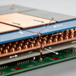
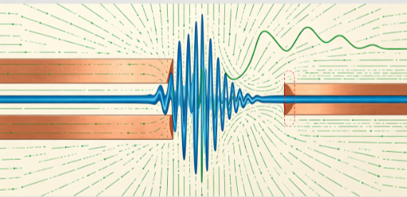
When a signal trace crosses from one copper-thickness region to another, the conductor cross-section changes. This modifies the electric-field and magnetic-field distribution around the trace and can change the local characteristic impedance.
The resulting behavior depends on the complete stackup and geometry. A transition from 1 oz to 3 oz copper, for example, should not automatically be assumed to produce a specific impedance shift such as +12 Ω. The actual value must be determined through electromagnetic simulation and measurement.
2. Mechanism One: Changes in Effective Dielectric Environment
The first mechanism is the change in the electromagnetic field distribution around the conductor.
For a microstrip or stripline structure, the transmission-line impedance depends on the effective dielectric environment and conductor geometry. A simplified relationship is:
[
Z_0 \propto \frac{1}{\sqrt{\varepsilon_{eff}}}
]
where (Z_0) is characteristic impedance and (\varepsilon_{eff}) is the effective dielectric constant.
When conductor thickness changes, the field distribution near the conductor edges also changes. The amount of field interacting with the dielectric and surrounding conductors can therefore change.
However, it is not technically accurate to assume that increasing copper thickness always causes the same percentage increase in effective Dk or the same fixed impedance reduction.
The magnitude and direction of the impedance change depend on whether the structure is microstrip, stripline, embedded microstrip, or another geometry, as well as on trace width, dielectric thickness, copper profile, and reference-plane spacing.
For this reason, a PCB impedance calculation should use the actual cross-sectional geometry rather than a generic copper-thickness correction factor.
3. Mechanism Two: Electromagnetic Discontinuity at the Transition
The second mechanism is the localized discontinuity created by the geometry transition.
A uniform transmission line has relatively stable distributed capacitance and inductance per unit length. When the conductor geometry changes, these distributed parameters also change.
Conceptually:
[Z_0 \approx \sqrt{\frac{L’}{C’}}]
where (L’) and (C’) represent the distributed inductance and capacitance per unit length.
At a copper-thickness transition, both quantities can change locally. This creates a short impedance transition rather than a perfectly uniform transmission line.
The discontinuity can cause:
- Reflections
- Localized return loss degradation
- Additional insertion loss
- TDR impedance excursions
- Eye-diagram degradation
- Reduced signal-integrity margin
The important point is that this is fundamentally a signal integrity issue caused by a geometric discontinuity.
It should not automatically be described as ground bounce or ground bounce caused by a return-current event. The correct analysis is to examine the local electromagnetic structure and the continuity of the signal and return paths.
4. Return-Path Continuity Is Equally Important
The signal conductor cannot be evaluated independently from its return path.
A high-speed signal normally establishes a return current path in the nearest reference structure. If the reference plane is interrupted, narrowed, split, or significantly altered near the copper-thickness transition, the return current distribution may change.
This can increase the effective inductance of the transition and create additional reflection.
The reference plane should therefore remain as continuous as possible beneath or adjacent to the high-speed routing region.
When evaluating a copper-thickness transition, engineers should inspect both:
- The signal conductor geometry
- The return-path geometry
A transition that appears harmless when viewed only from the signal layer may become a significant discontinuity when the entire signal-return structure is considered.
5. Why Skin Depth Is Usually Not the Primary Explanation
High-frequency conductor loss is influenced by skin effect, copper roughness, conductor thickness, and proximity effects.
The skin depth of copper can be approximated by:
[\delta = \sqrt{\frac{2\rho}{\omega\mu}}]
At approximately 2 GHz, the skin depth of copper is on the order of a few micrometers, depending on the assumptions used.
Because standard 1 oz and 3 oz copper are substantially thicker than the skin depth at this frequency, the difference in bulk copper thickness does not simply translate into a proportional change in skin depth.
However, this does not mean copper thickness has no high-frequency effect.
Copper thickness can still influence:
- Conductor geometry
- Current distribution
- Edge-field distribution
- Trace resistance
- Surface roughness contribution
- Proximity effects
- Local impedance
Therefore, it is better to distinguish between PCB impedance discontinuity caused by geometry and high-frequency conductor-loss mechanisms caused by skin and proximity effects.
6. TDR Testing Can Reveal the Transition
TDR testing is particularly useful for identifying localized impedance discontinuities.
A TDR instrument sends a fast electrical transition through the transmission line and observes reflections caused by changes in impedance. The resulting waveform can help engineers identify the approximate location and magnitude of discontinuities.
For a copper-thickness transition, engineers should compare:
- Uniform-copper reference structures
- Copper-thickness transition structures
- Different transition geometries
- Different trace widths
- Different reference-plane configurations
The TDR result should then be correlated with the physical location of the transition.
A measured impedance peak or dip should not automatically be attributed to copper thickness. Connectors, vias, test fixtures, solder structures, surface finishes, and calibration errors can also generate TDR features.
A proper test structure is therefore essential.
7. Why a Single 2D Cross-Section May Not Be Enough
A conventional field solver can accurately analyze a uniform PCB cross-section when the geometry is constant along the propagation direction.
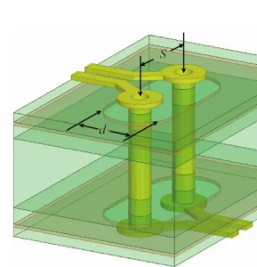
However, a copper-thickness transition is a three-dimensional structure.
If the trace changes from one conductor thickness to another over a finite distance, the electromagnetic fields around the transition vary along the signal-propagation direction.
Therefore, relying only on one uniform 2D cross-section can miss important transition behavior.
For critical high-speed PCB designs, engineers should consider:
- Multiple cross-sectional models
- 3D electromagnetic simulation
- Transition geometry
- Signal and return paths
- Via structures
- Copper step geometry
- Local dielectric variation
A practical simulation workflow can analyze the uniform sections first and then model the transition region separately.
This provides a more realistic understanding of the impedance discontinuity.
8. Avoid Universal Copper-Thickness Rules
It may be tempting to establish a simple rule such as:
“Never allow a 1 oz to 3 oz transition.”
Such a rule can be useful as an internal design guideline for a particular manufacturing process, but it should not be treated as a universal high-speed PCB requirement.
Whether a copper-thickness transition is acceptable depends on:
- Target impedance
- Data rate and signal spectrum
- Rise/fall time
- Transition length
- Trace geometry
- Dielectric thickness
- Reference-plane structure
- Channel loss budget
- Allowable reflection
- Receiver tolerance
- Manufacturing capability
A relatively large copper-thickness difference may be acceptable in one geometry but problematic in another.
Likewise, a small thickness difference can still create an issue if the transition occurs in an extremely sensitive high-speed channel.
The correct approach is therefore to define an allowable impedance-discontinuity budget for the specific design.
9. Design Strategies for Copper-Thickness Transitions
When a high-speed trace must cross a copper-thickness boundary, several design strategies can reduce the discontinuity.
Strategy 1: Avoid the Transition
The simplest solution is to route critical high-speed signals entirely within a region with consistent copper thickness.
This eliminates one major source of geometric discontinuity.
Strategy 2: Use a Controlled Transition
If crossing the boundary is unavoidable, the conductor geometry can be gradually transitioned instead of changing abruptly.
Possible approaches include:
- Tapered trace geometry
- Controlled copper step structures
- Local copper-thickness adjustment
- Dedicated transition zones
The exact geometry should be developed together with the PCB fabricator because the achievable dimensions depend on the manufacturing process.
Strategy 3: Maintain Reference-Plane Continuity
The reference plane should remain continuous around the transition whenever possible.
Avoid unnecessary plane voids, splits, neck-down regions, and abrupt return-path changes near the critical signal.
Strategy 4: Optimize the Transition in Simulation
For high-speed links, engineers can sweep:
- Trace width
- Transition length
- Copper thickness
- Dielectric thickness
- Trace-to-plane spacing
- Taper geometry
The objective is not necessarily to make the transition physically invisible. Instead, the goal is to keep the resulting reflection within the system’s signal integrity budget.
10. Surface Finish and Other Secondary Effects
Surface finish can also contribute to high-frequency behavior, particularly when conductor dimensions become small relative to the signal wavelength and skin depth.
For example, ENIG introduces nickel and gold layers over the copper surface. At high frequencies, the electrical properties and thickness of these layers can influence conductor loss and electromagnetic behavior.
However, assigning a universal impedance increase to ENIG based on a fixed nickel permeability value is not appropriate. The actual effect depends on nickel composition, thickness, frequency, geometry, and the electromagnetic model.
Therefore, surface finish should be included in detailed modeling when the application has very tight loss or impedance requirements.
11. Practical Verification Workflow
For a critical high-speed design, the following workflow can help identify copper-thickness-related problems before mass production.
Step 1: Map copper thickness
Identify all regions using different copper weights, including signal layers and relevant plane structures.
Step 2: Mark critical crossings
Identify every high-speed trace that crosses a copper-thickness boundary.
Step 3: Extract the actual geometry
Record trace width, copper thickness, dielectric thickness, reference-plane spacing, and transition length.
Step 4: Simulate the uniform sections
Determine the nominal impedance of each uniform region.
Step 5: Model the transition
Use a suitable 3D or transition-aware electromagnetic model for critical structures.
Step 6: Build a test coupon
Include uniform sections and representative copper-thickness transitions in the coupon.
Step 7: Perform TDR testing
Use calibrated TDR testing to locate and quantify impedance discontinuities.
Step 8: Perform system-level validation
Evaluate eye diagrams, insertion loss, return loss, and bit-error performance where appropriate.
Step 9: Review manufacturing capability
Confirm that the proposed copper transition can be manufactured consistently and that the actual production geometry matches the simulation assumptions.
12. The Key Principle: Copper Thickness Is a Geometric Variable
For high-speed PCB design, copper thickness should not be considered only as a material specification such as “1 oz” or “3 oz.”
It is also a geometric variable that influences the transmission-line structure.
When a signal crosses a copper-thickness boundary, the local electromagnetic environment changes. The resulting PCB impedance variation can create an impedance discontinuity, reflections, and reduced signal integrity margin.
The solution is not to impose one universal copper-thickness rule. Instead, engineers should identify critical transitions, maintain the reference plane, model the actual three-dimensional structure, and verify the design with TDR testing and representative prototypes.
For demanding high-speed PCB applications, early coordination between PCB design, SI engineering, simulation teams, and manufacturing engineers can prevent a small geometric transition from becoming a system-level signal-integrity problem.
Kingda can support impedance-controlled PCB fabrication, high-speed PCB manufacturing, and prototype verification, helping engineers evaluate copper-thickness transitions and maintain consistent production performance.