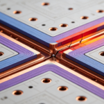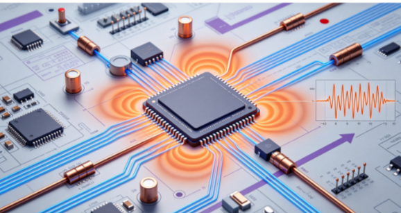
When a BGA device powers up and multiple I/O signals switch simultaneously, a short-duration voltage spike may appear on the power or ground pins. In severe cases, the transient can disturb the power-on-reset circuit and cause an unexpected system reset.
Interestingly, two identical ICs on the same PCB can behave differently. One device may operate normally while another experiences a reset. The difference may come from the local power-distribution network (PDN), especially the physical layout of the decoupling capacitor routing.
A decoupling capacitor can have the correct capacitance, low ESR, and excellent electrical specifications, yet still provide limited high-frequency protection if its connection to the IC and reference plane contains excessive inductance.
The key issue is therefore not simply capacitor value. It is the complete high-frequency current loop formed by the IC, capacitor, vias, power plane, and ground plane.
Ground Bounce Is Mainly a Transient Inductance Problem
Ground bounce is a transient voltage disturbance caused by rapid changes in current through parasitic inductance.
A simplified relationship is:
V = L × di/dt
where:
- V is the transient voltage
- L is the effective loop inductance
- di/dt is the rate of current change
When an I/O driver switches rapidly, the current can change within a very short time. If the current return path contains significant inductance, even a small amount of inductance can generate a noticeable transient voltage.
This is why return path design becomes increasingly important as signal edge rates become faster.
The effective current loop may include:
IC power or ground connection → package interconnect → PCB via → power/ground plane → decoupling capacitor → capacitor terminals → PCB via → IC power connection.
The exact loop depends on the package structure and PCB stackup.
Therefore, engineers should not evaluate inductance based only on the nominal ground-plane structure. The physical geometry of the complete high-frequency current path is what determines the effective loop inductance.
Why Decoupling Capacitor Routing Matters
The purpose of a decoupling capacitor is to provide a low-impedance local current source for high-frequency transient demand.
When an IC switches, the capacitor should supply the transient current through the shortest practical path.
If the capacitor is connected through a long trace or a distant ground via, the parasitic inductance increases. The capacitor may still have the correct nominal capacitance, but its high-frequency effectiveness can be significantly reduced.
This is the central reason why decoupling capacitor routing should be treated as part of the power-distribution design rather than ordinary signal routing.
A simplified current path is:
IC power pin → short copper connection → capacitor → short ground connection → ground plane → IC
The shorter and wider this high-frequency loop is, the lower its parasitic inductance generally becomes.
However, trace length alone is not sufficient to predict performance. Via geometry, plane spacing, current spreading, package inductance, capacitor mounting geometry, and the return-current path must also be considered.
The Complete Loop Inductance Determines Transient Noise
Loop inductance is one of the most important parameters in high-speed decoupling design.
It is influenced by:
- Trace length
- Trace width
- Via structure
- Via-to-pad distance
- Power/ground plane spacing
- Current-loop area
- Capacitor package size
- Capacitor pad geometry
- IC package inductance
- Reference-plane continuity
- Return-current distribution
For example, moving a ground via farther away from the capacitor ground pad increases the physical loop area. This generally increases parasitic inductance.
Similarly, routing the capacitor through a narrow dogbone trace can introduce additional inductance compared with placing the via directly adjacent to the pad.
There is no universal inductance increase for every 0.5 mm of additional distance because the result depends strongly on the PCB stackup and geometry. Any numerical value should therefore be treated as a measured or simulated result for a specific construction.
Why Capacitor Value Is Not the Only Important Parameter
A common layout mistake is to focus heavily on capacitance and ESR while ignoring the physical connection.
Suppose two 0.1 μF ceramic capacitors have similar capacitance, dielectric, and ESR. One is placed close to the IC with short connections to power and ground, while the other is several millimeters away.
At low frequencies, both capacitors may appear electrically similar.
At higher frequencies, however, the parasitic inductance of the PCB connection and component package becomes increasingly important.
The capacitor’s effective impedance can be approximated by:
Z ≈ ESR + jωL + 1/(jωC)
As frequency increases, the inductive term becomes more significant. Eventually, the capacitor no longer behaves as an ideal capacitor.
This explains why a larger capacitance does not automatically provide better high-frequency decoupling.
Edge Rate Is More Important Than Clock Frequency
When evaluating transient noise, engineers should pay close attention to signal rise time (tr) rather than relying only on the nominal clock frequency.
A relatively low-frequency digital signal can still generate high-frequency spectral components if its transition edge is very fast.
For this reason, high-speed PCB power integrity should be evaluated according to the actual edge rate, simultaneous switching activity, package characteristics, and PDN response.
A practical engineering approach is:
- Very fast edges: minimize capacitor-to-via and capacitor-to-device distances and reduce loop area aggressively.
- Moderate-speed digital interfaces: optimize local decoupling placement and verify PDN impedance.
- Slower interfaces: slightly longer connections may be acceptable, but the complete PDN should still be checked.
Specific limits such as 1.5 mm, 2.3 mm, or 3.5 mm should not be treated as universal design standards. The acceptable routing distance depends on the target impedance, edge rate, current transient, PCB stackup, and component package.
Keep the Ground Connection Short and Direct
For high-frequency decoupling, the capacitor ground terminal deserves the same attention as its power terminal.
A common mistake is to place the power via close to the capacitor but route the ground connection through a longer path.
This creates an asymmetric current loop.
A better arrangement is to place the power and ground connections close to the corresponding capacitor pads whenever the stackup permits it.
For 0402 or 0201 capacitors, direct-via or via-in-pad structures may provide very low-inductance connections when supported by the manufacturing process.
For larger packages, multiple vias can reduce current crowding and lower effective connection impedance.
The exact via diameter, number of vias, and via-to-pad distance should be determined according to the manufacturer’s capabilities and the required current and impedance performance.
Avoid Splits in the High-Frequency Return Path
The capacitor ground connection should not cross a plane split, void, or unnecessary anti-pad region.
If the return current is forced to detour around a discontinuity, the current-loop area increases.
This can increase:
- Loop inductance
- PDN impedance
- Ground noise
- Electromagnetic coupling
- Voltage transient amplitude
This is particularly important for BGA devices because many power and ground connections are concentrated within a relatively small area.
A continuous reference plane beneath the device and local decoupling network can provide a much more controlled return path.
Do Not Move All Decoupling Capacitors to the PCB Backside
Placing capacitors on the back side of a PCB can be useful when the BGA escape area is crowded. However, backside placement should not automatically be considered equivalent to top-side placement.
The additional vias required to connect the capacitor to the IC power and ground structures can add parasitic inductance.
The correct question is not:
“Is the capacitor close to the IC?”
It is:
“How long and inductive is the complete current loop between the capacitor and the IC?”
A backside capacitor can still perform well if the via structure and stackup provide a short, low-inductance path. Conversely, a capacitor located physically close to the IC may perform poorly if it is connected through long traces and multiple unnecessary vias.
Power Integrity and PDN Impedance
The effectiveness of local decoupling should ultimately be evaluated from the perspective of power integrity.
A useful concept is target PDN impedance:
Ztarget ≈ ΔV / ΔI
where ΔV is the allowable voltage fluctuation and ΔI is the expected transient current.
For example, if a processor power rail must remain within a certain voltage tolerance during a specified transient current change, the PDN must maintain sufficiently low impedance over the relevant frequency range.
This impedance includes much more than the capacitor itself:
- Voltage-regulator output impedance
- PCB planes
- Power vias
- Capacitor ESL and ESR
- Package inductance
- IC power/ground connections
- Interconnect geometry
Therefore, simply adding more capacitors may not solve a high-frequency noise problem.
If all capacitors are connected through a high-inductance path, their theoretical capacitance may not be effectively available at the frequency where the transient occurs.
How to Optimize Decoupling Capacitor Placement
A practical decoupling capacitor routing strategy can follow several steps.
1. Identify the Fastest Current Transients
Determine which IC pins or interfaces generate the largest di/dt.
High-speed processors, FPGAs, SerDes devices, DDR interfaces, and large BGA devices can generate substantial transient current.
2. Place High-Frequency Capacitors Near the Relevant Power Pins
The capacitor should be positioned according to the actual current path rather than simply placed somewhere inside the BGA outline.
The shortest physical distance is not always the shortest electrical path.
3. Minimize Current-Loop Area
Keep power and ground connections close together.
Avoid long parallel traces, unnecessary neck-down regions, and unnecessary via transitions.
4. Maintain a Continuous Reference Plane
Ensure that the high-frequency return current has a low-impedance path back to the IC.
5. Verify the PDN
Use impedance analysis or PI simulation to determine whether the local decoupling network meets the required impedance across the relevant frequency range.
Common Layout Pitfalls
Several mistakes repeatedly appear in high-speed PCB designs.
Pitfall 1: Choosing capacitors only by capacitance
A 0.1 μF capacitor is not automatically better than a 0.047 μF capacitor. Package size, ESL, mounting geometry, and connection inductance can be equally important.
Pitfall 2: Using long dogbone traces
Dogbone fanout can be convenient for BGA routing, but it adds connection length and therefore parasitic inductance.
Pitfall 3: Placing the ground via too far away
The capacitor may look close to the IC while its actual high-frequency return path remains long.
Pitfall 4: Ignoring the backside via path
A backside capacitor can introduce additional vertical interconnect inductance.
Pitfall 5: Crossing plane discontinuities
A split reference plane can force return current to take a longer path and increase loop inductance.
Pitfall 6: Adding capacitors without analyzing the PDN
More capacitance does not necessarily mean lower impedance across the entire frequency range.
A Practical Verification Method
When a high-speed BGA design experiences unexpected power or ground noise, engineers can use the following troubleshooting sequence:
- Measure the voltage transient directly at the IC power/ground reference.
- Check whether multiple I/O outputs switch simultaneously.
- Inspect the capacitor-to-pad and capacitor-to-via distances.
- Identify the complete current return path.
- Check for plane splits or reference discontinuities.
- Review package and via inductance.
- Perform power integrity or PDN impedance simulation.
- Compare different capacitor placements experimentally.
- Verify the result with an oscilloscope using an appropriate probing technique.
Probe selection is particularly important. A long oscilloscope ground lead can itself introduce inductance and create an apparent ringing or voltage spike that is not representative of the actual PCB behavior.
For high-speed measurements, a spring ground, coaxial connection, or suitable low-inductance probing method can provide more reliable results.
How Kingda Can Help Optimize High-Speed PCB Power Distribution
At Kingda, high-speed PCB power integrity should be considered from the schematic and stackup stages through PCB layout, manufacturing, and validation.
For BGA-based designs, engineers can evaluate:
- Decoupling capacitor placement
- Power and ground via arrangement
- Stackup and plane spacing
- Return-path continuity
- BGA breakout routing
- PDN impedance
- Loop inductance
- Manufacturing constraints
- Prototype measurement results
The key principle is simple: a decoupling capacitor is only as effective as the high-frequency current path connecting it to the IC.
When edge rates become faster, reducing loop inductance and maintaining a continuous return path often matters more than simply increasing capacitance.
By optimizing decoupling capacitor routing, loop inductance, return path, and PDN impedance together, engineers can reduce transient noise and improve the power integrity and reliability of high-speed PCB systems.