A high-speed server PCB can pass signal integrity simulation and still experience unexpected failures during laboratory testing. One common cause is power plane resonance, which can create localized voltage fluctuations in the power distribution network (PDN) and indirectly disturb high-speed signal paths.
During the debugging of an 8-layer server board, for example, a DDR5 interface showed significant eye-diagram degradation at a high data rate. Network-analyzer measurements identified an impedance anomaly in the power distribution network around a specific frequency. When a probe was placed near a decoupling capacitor, the observed jitter changed noticeably.
This type of behavior is not necessarily a signal-routing problem. It can occur because resonance in the power and ground structure changes the local reference environment and introduces noise into sensitive signal paths.
The key engineering question is therefore not simply whether the power plane resonates, but how the resonant energy couples into the signal system.
What Is Power Plane Resonance?
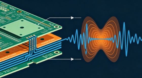
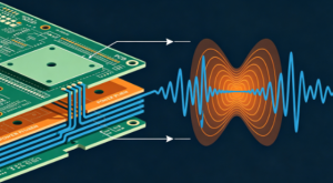
In a multilayer PCB, power and ground planes form a distributed electromagnetic structure. The dielectric material between the planes provides capacitance, while current paths and plane geometry contribute inductance.
Together, these structures can form distributed resonant modes.
At certain frequencies, the impedance of the power distribution network can increase sharply. A transient current flowing through this higher impedance can produce a larger local voltage disturbance:
ΔV(f) = Itransient(f) × ZPDN(f)
where:
- ΔV is the local power or reference-plane voltage disturbance
- Itransient is the transient current component
- ZPDN is the frequency-dependent PDN impedance
When PDN impedance rises around a resonant frequency, even a relatively small transient current can produce a measurable voltage fluctuation.
The result may appear as power noise, reference-plane movement, common-mode noise, or signal jitter.
How Does Power Plane Resonance Become Signal Interference?
There are two major coupling mechanisms that engineers should examine.
1. Plane Resonance Changes the Local Return-Current Environment
High-speed signals require a controlled electromagnetic return path. The return current normally follows the path of lowest impedance around the signal conductor, strongly interacting with the adjacent reference plane.
When a power or ground structure enters resonance, its voltage and current distribution become nonuniform.
Instead of behaving like an ideal low-impedance reference, part of the plane can develop localized voltage maxima and minima.
This can produce:
- Local reference-voltage variation
- Increased return-path impedance
- Additional loop inductance
- Impedance discontinuities
- Differential-to-common-mode conversion
- Increased coupling between neighboring structures
For a high-speed interface, the reference conductor is part of the transmission system. Therefore, noise on that reference structure can directly affect the measured signal.
This is why signal integrity problems sometimes appear even when the signal trace itself has not been changed.
2. PDN Resonance Creates Common-Mode Noise
A second mechanism is common-mode coupling.
Suppose a processor, memory device, FPGA, or ASIC produces a fast transient current. If the PDN impedance is low, the resulting voltage disturbance remains relatively small.
At a resonant frequency, however, the PDN impedance can increase significantly.
The resulting voltage fluctuation can couple through:
- Package structures
- Power and ground vias
- Decoupling capacitors
- Reference planes
- Connector structures
- Parasitic capacitance
- Shared return paths
Some of this energy can appear as common-mode voltage on high-speed interfaces.
For differential signaling, this is particularly important. Differential signaling provides strong rejection of common-mode noise under ideal conditions, but real systems have finite common-mode conversion caused by package asymmetry, via transitions, reference-plane discontinuities, connector imbalance, and other nonidealities.
Consequently, power-plane noise can eventually appear as differential signal degradation.
Why the Resonant Frequency Is Not Determined by Plane Length Alone
A common simplified model relates plane dimensions to electromagnetic wavelength:
λ ≈ c / (f√Dk)
This relationship can provide intuition, but it should not be treated as a universal formula for predicting a PCB resonance frequency.
Actual power plane resonance depends on many parameters, including:
- Plane length and width
- Plane shape
- Dielectric thickness
- Dielectric constant
- Dielectric loss
- Power and ground geometry
- Via locations
- Component connections
- Plane openings
- Decoupling capacitor locations
- Boundary conditions
- Package and connector structures
For example, a rectangular plane can support several resonant modes rather than a single resonance determined by its longest dimension.
In addition, a practical PCB rarely behaves like an isolated pair of ideal rectangular plates. Vias, component pads, anti-pads, cutouts, connectors, and neighboring planes modify the electromagnetic field.
Therefore, plane dimensions should be used as an initial diagnostic clue rather than as the final design criterion.
Why Decoupling Capacitors May Not Solve the Problem
A common reaction to PDN resonance is to add more capacitors.
However, simply increasing the capacitor count does not guarantee lower impedance across the entire frequency range.
A practical capacitor can be represented by:
Z ≈ ESR + jωESL + 1/(jωC)
At low frequencies, capacitance dominates.
As frequency increases, ESL becomes increasingly important. Eventually, the capacitor reaches its self-resonant region, after which its impedance begins to increase.
Therefore, several capacitors with identical values and packages may provide limited additional benefit at a particular high-frequency resonance.
Effective PDN design requires a combination of:
- Appropriate capacitance values
- Low-ESL packages
- Short current paths
- Proper power/ground via placement
- Low-inductance plane connections
- Distributed capacitor placement
- Appropriate VRM-to-load impedance control
The objective is to control the PDN impedance over the relevant frequency range rather than simply maximize the number of capacitors.
Why Capacitor Placement Near the BGA Matters
For high-speed processors and memory devices, the distance between the power pins, decoupling capacitors, and reference planes can strongly influence the high-frequency current loop.
A capacitor located far from the device may still provide useful low-frequency energy storage, but its parasitic inductance can limit its effectiveness at higher frequencies.
The relevant current loop includes:
Device power pin → capacitor → ground connection → reference plane → device ground path
Every additional via, trace segment, neck-down region, or unnecessary transition can contribute inductance.
For this reason, high-frequency decoupling capacitors are often placed close to the device power and ground connections.
However, the exact placement should be determined by the package escape structure, stackup, via arrangement, capacitor package, target impedance, and measured PDN behavior rather than by a universal distance rule.
Cutting the Plane Is Not Always an Effective Fix
One proposed solution for a resonant power plane is to introduce a slot or isolation region.
A slot can change the resonant modes by modifying the plane geometry, but it can also introduce additional inductance and disrupt current distribution.
This creates a potential trade-off:
Resonance frequency shift ≠ resonance problem solved
A design modification that moves the resonance from one frequency to another may actually make the system worse if the new resonance has a higher impedance peak or falls closer to an important signal harmonic.
Therefore, engineers should compare at least:
- Resonant frequency
- Peak impedance
- PDN impedance across the operating band
- Voltage noise
- Signal jitter
- Eye opening
- Return-path continuity
- EMI behavior
A lower resonance peak with better impedance control can be more valuable than simply moving the resonance outside the original measurement point.
Using Additional Copper to Control Resonance
Adding copper can sometimes modify the plane capacitance and electromagnetic field distribution, particularly when the added copper forms part of a controlled power-ground structure.
However, the effect depends strongly on geometry.
A copper patch does not automatically behave as an ideal capacitor. Its effectiveness depends on:
- Copper area
- Distance to the reference plane
- Dielectric thickness
- Connection points
- Current path
- Via inductance
- Plane boundary conditions
For this reason, statements such as “every additional square centimeter lowers the resonant frequency by a fixed amount” should not be treated as universal design rules.
The better approach is to compare the complete PDN impedance before and after the modification.
Three Practical Steps for Diagnosing Power Plane Resonance
Step 1: Measure the PDN Impedance
Use a VNA or an appropriate impedance-measurement setup to identify peaks and anti-resonances in the PDN.
Measurement fixtures and calibration are critical because the connection between the instrument and PCB can introduce significant parasitic inductance.
The goal is to identify frequencies where the PDN impedance becomes unexpectedly high.
Step 2: Correlate the Resonance With the PCB Stackup
Review:
- Power-plane dimensions
- Ground-plane locations
- Dielectric thickness
- Dk and Df
- Plane openings
- Via fields
- BGA power connections
- Decoupling capacitor locations
This helps determine whether the measured resonance is associated with a plane mode, capacitor anti-resonance, via structure, or another part of the PDN.
Step 3: Correlate PDN Noise With Signal Degradation
Measure the power or reference-plane noise while simultaneously observing the high-speed interface.
Useful measurements may include:
- Eye diagram
- Jitter
- Differential voltage
- Common-mode voltage
- TDR
- S-parameters
- PDN impedance
- Near-field EMI scanning
If signal degradation changes significantly when the PDN impedance is modified, the electrical correlation provides much stronger evidence than relying on frequency coincidence alone.
Common Design Mistakes
Mistake 1: Checking Only DC Voltage Drop
A DC analysis can show that the power network has acceptable resistance and voltage drop.
However, PDN impedance is frequency dependent.
A power network can have excellent DC performance while exhibiting a high impedance peak at a specific AC frequency.
Therefore, DC IR-drop analysis and AC PDN analysis should be treated as complementary methods.
Mistake 2: Adding More Capacitors Without Studying Anti-Resonance
More capacitors can sometimes introduce additional impedance peaks because different capacitor values, ESRs, ESLs, and mounting structures interact.
The correct objective is not “more capacitance,” but a controlled impedance profile over the frequency range of interest.
Mistake 3: Moving the Resonance Without Checking the New Peak
Changing plane dimensions or adding slots may shift a resonance.
But if the resulting peak impedance becomes higher, the modification may worsen power noise.
Always compare both resonance frequency and impedance magnitude.
Mistake 4: Ignoring High-Frequency Return Paths
A power-plane modification may unintentionally interrupt the return path of nearby signals.
This can introduce a new PCB signal integrity problem even if the original PDN resonance is reduced.
Practical Design Guidelines
For high-speed multilayer PCBs, engineers can reduce resonance-related risk by following a structured design process:
- Keep power and ground structures well defined.
- Minimize unnecessary plane discontinuities.
- Place low-ESL decoupling capacitors close to high-current transient loads.
- Minimize power/ground via-loop inductance.
- Use a continuous reference plane for critical high-speed signals whenever possible.
- Evaluate capacitor anti-resonance rather than capacitance alone.
- Include stackup tolerances in PDN and SI analysis.
- Validate critical designs with impedance measurements.
- Correlate PDN noise with eye diagrams and jitter.
- Perform EMC measurements when power-plane noise may contribute to radiated or conducted emissions.
How Kingda Can Help With PDN and PCB Design Validation
At Kingda, PCB design evaluation can consider the electrical relationship between the stackup, power distribution network, reference planes, vias, and high-speed signal routing.
For designs with strict SI/PI or EMI requirements, the engineering process can include:
- Stackup review
- Power and ground plane analysis
- Decoupling strategy review
- High-speed return-path analysis
- DFM review
- Prototype validation
- Impedance testing
- Cross-section inspection
- EMI troubleshooting support
The goal is not simply to eliminate one measured resonance. It is to establish a stable power and reference structure that remains compatible with the complete high-speed system.
Conclusion
Power plane resonance is not merely a power-integrity problem. In a high-speed multilayer PCB, resonant PDN behavior can create local voltage fluctuations, disturb reference potentials, modify return-current paths, and introduce common-mode coupling.
The resulting effects may appear as:
- Eye-diagram closure
- Increased jitter
- Impedance discontinuity
- Common-mode noise
- Crosstalk
- EMI interference
- Intermittent high-speed communication failures
The most effective troubleshooting method is to establish an electrical correlation between PDN impedance, plane behavior, reference noise, and signal degradation.
Rather than relying on a single plane-dimension formula or adding capacitors blindly, engineers should evaluate the complete stackup and PDN structure through simulation, measurement, and prototype validation.
A stable power distribution network is therefore an essential part of reliable high-speed PCB design and overall PCB signal integrity.