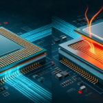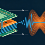
During an EMI interference investigation for a power electronics PCB, a noticeable emission increase was observed around 300 MHz. Cross-sectional analysis revealed a small copper area on an inner layer that was electrically floating and positioned very close to an adjacent signal trace.
This type of structure is often overlooked because it does not appear to be connected to any active circuit. However, an electrically floating copper area can behave as a passive capacitive structure. When it is located between or near a signal trace and a reference plane, transient electric fields can induce voltage on the copper and provide an unintended path for high-frequency current.
The problem is therefore not simply whether the copper is connected at DC. The more important question is how the floating structure interacts with the signal field, reference plane, stackup, and return-current path.
What Is Isolated Copper on an Inner PCB Layer?
Isolated copper refers to a copper region on a PCB layer that has no intentional electrical connection to a defined net, such as GND or a power rail.
Small isolated copper areas can be created unintentionally during PCB layout. Typical causes include:
- Copper pours surrounding traces
- Unused copper remaining after routing
- Thermal relief or clearance regions
- Copper remnants created during layer editing
- Local plane shapes that are not connected to a valid net
- Copper structures left after design changes
On an inner layer, the situation can be more complicated because the copper is embedded between dielectric layers. It may therefore be electrically invisible during a basic DC continuity check while still interacting strongly with nearby high-speed signals.
For this reason, PCB design reviews should evaluate not only DC connectivity but also the physical relationship between floating copper, signal traces, and reference planes.

Why Can Floating Copper Cause Coupling Interference?
The first major mechanism is capacitive coupling.
Consider an inner-layer floating copper region positioned close to a signal trace. The signal trace and floating copper form a parasitic capacitance. The floating copper also has capacitance to the nearby PCB ground plane or other reference conductor.
A simplified equivalent structure can be represented as:
Signal trace → parasitic capacitance → floating copper → parasitic capacitance → reference plane
When the voltage on the signal trace changes rapidly, displacement current can flow through these parasitic capacitances.
The basic relationship is:
i = C × dv/dt
This means that faster voltage transitions and larger parasitic capacitance can produce greater transient current.
The effect becomes more noticeable as the distance between the floating copper and signal trace decreases. Copper area, dielectric thickness, dielectric constant, trace geometry, and the relative position of the reference plane all influence the resulting capacitance.
Consequently, simply measuring whether the floating copper has a DC connection does not reveal its high-frequency behavior.
The Role of the Reference Plane and Return Path
A second important factor is the return path.
High-speed signals do not propagate through a PCB as isolated traces. Their electromagnetic fields interact with nearby reference conductors, and the associated return current tends to follow a path that minimizes impedance and loop inductance.
If an isolated copper region is placed close to a signal trace, it can disturb the local field distribution. Depending on the stackup and geometry, the floating copper may:
- Alter the local electric field
- Increase parasitic capacitance
- Modify local impedance
- Redistribute return current
- Increase common-mode conversion
- Couple noise into adjacent structures
This is particularly important in high-speed PCB designs where signal edges contain substantial high-frequency energy even when the nominal clock or data frequency appears relatively low.
A differential pair, for example, can tolerate some common-mode disturbance under certain conditions, but an asymmetric floating structure can disturb the balance between the two conductors. This can increase differential-to-common-mode conversion and potentially contribute to EMI interference.
Why the Physical Size of the Copper Matters
The physical dimensions of an isolated copper region influence its parasitic capacitance and electromagnetic behavior, but there is no universal copper-area threshold that determines whether interference will occur.
A larger copper area generally provides greater coupling area and therefore can produce stronger capacitive interaction when positioned close to a signal conductor.
However, area alone is not enough to determine the risk.
The following parameters should be considered together:
| Parameter | Potential Effect |
|---|---|
| Copper area | Influences coupling capacitance |
| Distance to signal trace | Smaller distance generally increases coupling |
| Distance to reference plane | Changes field distribution and capacitance |
| Dielectric thickness | Affects electric-field confinement |
| Dielectric constant | Influences parasitic capacitance |
| Signal edge rate | Faster transitions increase displacement current |
| Copper geometry | Affects field distribution |
| Reference-plane continuity | Determines the available return path |
| Trace impedance | Can change local reflection behavior |
Therefore, a 2 mm² floating copper area in one stackup may have little practical impact, while a smaller structure placed extremely close to a sensitive high-speed trace could still become relevant.
Do Not Treat Copper Size as the Only Resonance Criterion
The original assumption that the copper length alone determines a quarter-wavelength resonance is too simplistic for multilayer PCB structures.
An isolated copper region embedded in a multilayer stackup is not necessarily a conventional quarter-wave antenna. Its electromagnetic behavior depends on its shape, surrounding reference planes, dielectric thickness, excitation mechanism, boundary conditions, and nearby structures.
At sufficiently high frequencies, local copper geometry can participate in resonant or cavity-like behavior. However, identifying a specific resonance frequency requires electromagnetic analysis or measurement rather than applying a single wavelength rule.
For practical PCB signal integrity analysis, the first priority should therefore be identifying the coupling path and determining whether the floating copper is altering the local field or return-current distribution.
Why High-Frequency Materials Can Produce Unexpected Results
Changing the PCB laminate does not automatically eliminate coupling problems.
Materials with lower dielectric loss can reduce dielectric attenuation, but that does not mean every unwanted coupling mechanism becomes weaker.
A lower-loss dielectric may allow electromagnetic energy to propagate with less attenuation. If the geometry already creates an unwanted coupling path, reducing dielectric loss can sometimes make the disturbance more visible at the receiving structure.
This is why material selection should not be separated from layout analysis.
For a high-frequency design, engineers should evaluate:
- Dk and Df
- Dielectric thickness
- Copper roughness
- Trace geometry
- Reference-plane spacing
- Signal edge rate
- Coupling distance
- Return-path continuity
- Connector and via transitions
Material selection and PCB design must be evaluated as a complete electromagnetic system.
Three Practical Ways to Deal With Isolated Copper
1. Remove Unnecessary Floating Copper
If an isolated copper area provides no electrical, thermal, or mechanical function, removing it is often the simplest solution.
This is especially useful when the copper is:
- Very close to a high-speed trace
- Located in a sensitive analog region
- Near an RF transmission line
- Positioned between a signal and its reference plane
- Located close to an EMI-sensitive circuit
Removing unnecessary copper eliminates the associated parasitic capacitance rather than attempting to control it later.
2. Connect Functional Copper to an Appropriate Net
If the copper region is intentionally required, connecting it to a suitable reference net can make its electrical behavior more predictable.
For example, a copper region that is intended to function as part of the ground structure should generally have a defined connection to the ground network rather than remain electrically floating.
However, adding a via does not automatically solve every problem.
The via location, connection inductance, nearby return path, and current-loop geometry all matter. A poor connection can still leave a substantial high-frequency impedance.
For this reason, PCB ground plane connections should be designed according to the actual current path rather than simply adding vias wherever convenient.
3. Increase the Separation From Sensitive Signals
If the copper cannot be removed or connected, increasing the clearance between the isolated copper and sensitive traces can reduce capacitive coupling.
This approach is particularly useful around:
- High-speed differential pairs
- RF traces
- High-impedance analog inputs
- Clock lines
- Switching-node signals
- Sensitive ADC/DAC interfaces
The required clearance should be established from the stackup, signal characteristics, impedance requirements, and EMC results rather than from one universal distance.
Common Mistakes in PCB Design
Mistake 1: Checking Only DC Connectivity
A multimeter may show that the copper is electrically isolated, but this does not mean that it is irrelevant at high frequency.
AC coupling occurs through parasitic capacitance even when there is no conductive DC path.
Therefore, PCB signal integrity analysis should consider both conductive and field-based coupling mechanisms.
Mistake 2: Assuming Thermal Changes Prove the Problem Is Gone
Heating a PCB and observing a temporary reduction in interference is not sufficient evidence that the isolated copper is harmless.
Temperature can change dielectric properties, material dimensions, copper geometry, and mechanical relationships simultaneously. The observed EMI change may therefore have multiple causes.
A controlled electrical and electromagnetic test is more reliable than a simple thermal experiment.
Mistake 3: Checking Only Outer-Layer Copper
A common CAM review focuses heavily on external copper pours while overlooking internal-layer copper structures.
Inner-layer copper is particularly important because it is embedded within the stackup and can be difficult to inspect after lamination.
Therefore, the PCB design review should include all signal, plane, and copper regions across the complete layer stack.
A Practical Inspection Workflow
For production PCB projects, the following workflow can help identify potentially problematic floating copper:
Step 1: Identify floating copper
Use CAM or PCB design software to generate a list of copper regions that are not assigned to a valid electrical net.
Step 2: Check their proximity to sensitive signals
Pay particular attention to floating copper located close to high-speed, RF, clock, analog, or switching-node traces.
Step 3: Review the complete stackup
Check the distance between the floating copper and adjacent signal/reference layers. Dielectric thickness can significantly affect parasitic coupling.
Step 4: Evaluate the return path
Determine whether the structure modifies the intended high-frequency return path or creates an asymmetric electromagnetic environment.
Step 5: Simulate or measure when necessary
For critical designs, use field-solver simulation, TDR, S-parameter measurements, near-field scanning, or EMC testing to determine whether the structure is actually contributing to the observed problem.

How to Reduce the Risk During PCB Manufacturing
Preventing floating copper problems is easier than attempting to correct them after fabrication.
A robust PCB manufacturing workflow should include:
- Complete inner-layer copper checks
- Net connectivity verification
- Minimum copper clearance verification
- Stackup review
- Reference-plane continuity checks
- CAM comparison against the released PCB data
- DFM review before fabrication
- Controlled engineering-change management
For high-volume production, the inspection criteria should also be standardized so that small changes to copper pours or internal planes do not introduce unintended floating structures.
Final Takeaway
An isolated copper region is not necessarily harmless simply because it has no DC connection.
In multilayer PCBs, isolated copper can interact with nearby signals through parasitic capacitance and can modify the local electromagnetic field and return path. Under certain conditions, this can contribute to common-mode noise, impedance discontinuities, crosstalk, and EMI interference.
The correct engineering approach is not to apply a universal copper-area rule. Instead, evaluate the copper area together with its distance from signals, dielectric structure, reference-plane geometry, signal edge rate, and overall PCB signal integrity requirements.
For critical designs, Kingda recommends reviewing internal copper topology during the stackup and CAM stages, removing unnecessary floating copper, defining appropriate reference connections, and validating suspected coupling paths through simulation and measurement.
A small piece of copper may appear electrically inactive, but at high frequency, its electromagnetic behavior can still become part of the circuit.