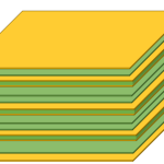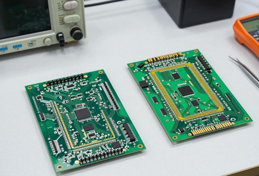
Many engineers evaluate redundant-layer reduction primarily from the perspective of material savings and lower PCB costs. However, its potential value extends beyond cost reduction. When properly engineered, reducing unnecessary layers can simplify the PCB manufacturing process, optimize the stackup, improve process stability, and reduce manufacturing risks during mass production.
For six-layer, eight-layer, and higher-layer boards, an unnecessarily complicated structure can increase the number of core and prepreg combinations, lamination interfaces, drilling requirements, and process tolerances. These factors may make manufacturing more difficult and increase the sensitivity of the process to material variation, registration errors, resin flow, warpage, and plated-hole quality.
However, it would be inaccurate to assume that a higher layer count automatically causes manufacturing defects. A well-designed high-layer-count board can be highly reliable, while an improperly optimized low-layer-count board can still experience significant problems.
Therefore, PCB layer reduction should be treated as a structured engineering optimization rather than simply deleting unused layers. The objective is to simplify the structure without compromising signal integrity, power distribution, mechanical performance, reliability, or manufacturing capability.
1. Manufacturing Risks Associated With Unnecessary PCB Layers
An unnecessarily complicated multilayer structure can increase manufacturing complexity in several ways.
Lamination Complexity
As layer count increases, the number and combination of core and prepreg materials can also increase. During lamination, resin flow, copper distribution, material thickness, registration, temperature, and pressure all influence the final board structure.
If the stackup is poorly balanced, potential problems can include:
- Interlayer registration variation
- Local resin starvation
- Voids
- Delamination
- Thickness variation
- Excessive board warpage
These problems are not caused by layer count alone. Stackup symmetry, copper distribution, material selection, lamination parameters, and supplier process capability must all be considered.
Board Warpage
An asymmetric PCB stackup can create uneven mechanical stress during lamination and subsequent thermal exposure.
Copper distribution is particularly important. If one side of the board contains significantly more copper than the other, thermal expansion and resin-flow behavior can become unbalanced.
During SMT reflow, additional thermal stress can amplify an existing mechanical imbalance and potentially affect:
- Component placement
- Solder-joint formation
- Connector alignment
- Mechanical assembly
- BGA reliability
Reducing unnecessary layers may simplify the structure, but the revised design still needs to maintain a mechanically balanced stackup.
Drilling and Plating Challenges
Higher-layer-count boards are often thicker and may require more demanding drilling and plating conditions. The relationship between finished board thickness and hole diameter determines the via aspect ratio.
A higher aspect ratio can make hole cleaning, desmear, copper deposition, and plating uniformity more challenging.
Potential defects include:
- Incomplete hole cleaning
- Uneven copper deposition
- Poor plating coverage
- Barrel cracks
- Intermittent electrical connections
After reducing layers, engineers should recalculate the finished thickness and via aspect ratio rather than assuming the original hole specifications remain appropriate.
Tolerance Accumulation
A multilayer PCB is a three-dimensional manufacturing structure. Variations in dielectric thickness, copper thickness, layer registration, etching, and lamination can accumulate throughout the board.
These variations can influence:
- Finished board thickness
- Controlled impedance
- Hole-to-copper clearance
- Registration accuracy
- Mechanical dimensions
Consequently, the purpose of layer reduction should not be to eliminate defects automatically, but to create a simpler and more controllable manufacturing structure.
2. DFM Principles for Reducing Redundant Layers
For mass production, DFM review should be performed before removing any layer.
Three principles are particularly important.
Principle 1: Maintain a Balanced and Manufacturable Stackup
After removing layers, the revised PCB stackup should be evaluated for symmetry and material compatibility.
Engineers should define:
- Core thickness
- Prepreg type and resin content
- Copper thickness
- Dielectric thickness
- Signal/reference-plane relationships
- Finished board thickness
- Controlled-impedance structures
A symmetrical structure is often beneficial for mechanical stability, but electrical requirements may sometimes require an intentionally asymmetric configuration. Therefore, symmetry should be considered together with electrical and manufacturing requirements rather than treated as an absolute rule.
Principle 2: Use Qualified Manufacturing Materials
Whenever possible, the revised design should use materials already qualified by the manufacturer.
This may include standard:
- Core materials
- Prepreg constructions
- Copper foils
- Surface finishes
- Via structures
- Lamination processes
Using qualified materials can reduce engineering setup and process-development requirements. However, material selection must still satisfy the electrical, thermal, and reliability requirements of the product.
Principle 3: Remove Only Genuine Redundancy
Not every lightly used layer is actually redundant.
Before deleting a layer, determine whether it provides:
- Signal routing capacity
- A reference plane
- A power-distribution function
- EMI shielding
- Return-current continuity
- Thermal conduction
- Mechanical balance
Unused signal layers, duplicate power regions, or unnecessary isolation structures may be candidates for optimization, but every proposed deletion should be evaluated against the complete electrical and physical design.
3. PCB Stackup Reconstruction After Layer Reduction
Once a layer has been identified as removable, the stackup must be rebuilt rather than simply deleting the corresponding layer from the CAD file.
The revised stackup should establish clear relationships between signal and reference layers.
For high-speed designs, engineers should check:
- Signal-to-reference-plane distance
- Differential-pair geometry
- Controlled impedance
- Return-current paths
- Via transitions
- Ground-plane continuity
For power circuits, the revised design should consider:
- Current-carrying capacity
- Plane resistance
- Power-loop inductance
- Decoupling
- Voltage drop
- Thermal distribution
For RF circuits, the stackup must also support stable transmission-line geometry and an appropriate electromagnetic reference environment.
After reconstruction, impedance should be recalculated using the actual dielectric thickness, copper thickness, Dk, trace width, and expected manufacturing tolerances.
4. Optimize PCB Layout and Power Distribution
Reducing layers usually means that some routing resources become more limited. Therefore, PCB process optimization should not be separated from layout optimization.
High-speed and sensitive signals should be reviewed first.
Engineers should identify:
- DDR and other high-speed buses
- Differential pairs
- Clock signals
- RF transmission lines
- Sensitive analog signals
- Switching power loops
- High-current paths
Where signals are moved to another layer, the return path must also be checked.
If a signal changes reference planes, appropriate ground stitching or return-path structures may be required. The exact solution depends on the stackup and signal characteristics.
Power and ground layers should also be reassessed. Combining power regions may reduce the number of layers, but excessive sharing can increase coupling or power-distribution impedance.
The optimized layout should therefore maintain adequate electrical separation while making efficient use of the remaining layers.
5. SI/PI Verification After Layer Reduction
After the revised layout and stackup are complete, electrical verification should be performed.
For high-speed designs, SI/PI simulation can be used to compare the original and revised configurations.
Typical parameters include:
- Single-ended impedance
- Differential impedance
- Eye diagram
- Insertion loss
- Return loss
- Crosstalk
- Overshoot and undershoot
- Jitter
- Timing margin
- PDN impedance
- DC voltage drop
The objective is not necessarily to make every parameter identical to the original design. Instead, the revised design should satisfy the product specification with sufficient engineering margin.
For lower-speed boards, a full SI/PI simulation may not be necessary, but power paths, grounding, signal coupling, and electrical continuity should still be reviewed.
6. DFM Review Before Prototype Production
A dedicated DFM review should be completed before the revised board enters fabrication.
The review should cover at least the following areas.
Stackup and Material Review
Verify that the new combination of core, prepreg, and copper foil is supported by the manufacturer’s qualified process.
Check:
- Material availability
- Finished thickness
- Dielectric thickness
- Copper balance
- Lamination compatibility
- Impedance requirements
Lamination Review
Evaluate potential risks related to:
- Resin flow
- Copper density
- Stackup symmetry
- Pressed thickness
- Registration
- Voids
- Delamination
- Warpage
Drilling and Plating Review
Recalculate:
- Hole aspect ratio
- Minimum hole diameter
- Annular ring
- Hole-to-copper clearance
- Via-to-trace spacing
- Plating requirements
The revised design should remain within the manufacturer’s qualified process window.
Documentation Review
All engineering documents must be updated together.
This includes:
- Stackup drawings
- Fabrication drawings
- Drill files
- Impedance specifications
- Material specifications
- PCB fabrication notes
- Assembly drawings
- Engineering change records
A common production failure occurs when the PCB database has been updated but the fabrication documents still contain the previous layer structure.
7. Representative Layer-Reduction Case Studies
Case 1: Eight-Layer Industrial Control Board
An eight-layer industrial board contained several lightly used signal layers and a duplicated ground structure. Instead of simply deleting the layers, the engineering team first reviewed signal routing, return paths, power distribution, and mechanical requirements.
The revised design consolidated the routing resources and rebuilt the stackup around the remaining functional layers.
The expected benefits included:
- Fewer lamination interfaces
- Simplified material management
- Reduced routing complexity
- Easier process control
- Potential reduction in manufacturing cost
Actual yield improvement and cost savings should be verified using pilot-production data rather than assumed in advance.
Case 2: Six-Layer Consumer Electronics Board
A six-layer board contained multiple low-voltage power regions that could be consolidated after a detailed electrical review.
The optimization process combined compatible power functions, removed unnecessary isolation structures, and reassigned signal routing.
After the redesign, the board required fewer layers and could potentially use a more standardized manufacturing process.
However, the key validation points remained signal integrity, power integrity, thermal performance, mechanical stability, and assembly compatibility.
These examples demonstrate that the value of layer reduction depends on the original design and manufacturing conditions. There is no universal percentage for cost or yield improvement.
8. Process Optimization After Layer Reduction
After the new layer structure has been approved, several manufacturing parameters should be reviewed.
Optimize Core and Prepreg Selection
Where possible, use qualified material families with compatible thermal and mechanical characteristics.
Avoid unnecessary combinations of different resin systems unless they are required by electrical or thermal performance.
The final selection should consider:
- Tg
- Td
- Z-axis CTE
- Dk/Df
- Moisture absorption
- Resin content
- Lamination behavior
Balance Copper Distribution
Copper balance should be reviewed across the complete stackup.
Large differences in copper density between the two sides of a board can contribute to:
- Warpage
- Resin-flow imbalance
- Uneven thermal behavior
Copper balancing should be performed without compromising signal integrity, impedance, thermal performance, or EMC requirements.
Recalculate Via Geometry
When the finished board becomes thinner, existing vias may have more favorable aspect ratios. Nevertheless, the hole diameter and plating specifications should be reviewed rather than changed automatically.
This can help align the design with standard drilling and plating processes.
Reduce Unnecessary Special Processes
If the revised design can eliminate unnecessary blind vias, buried vias, special lamination structures, or other advanced processes without compromising functionality, the manufacturing process may become simpler.
However, special processes should only be removed when they are genuinely redundant. Eliminating a process that serves an important electrical or mechanical function can create greater downstream risks than the original cost.
9. Pilot Production and Yield Optimization
After prototype validation, the revised design should move through a controlled pilot-production stage before full-scale mass production.
The pilot run should monitor actual PCB yield rather than relying solely on prototype results.
Recommended data points include:
- First-pass yield
- Board thickness distribution
- Warpage
- Impedance results
- Hole quality
- Lamination defects
- Surface-finish defects
- Assembly yield
- Functional-test results
Defect Pareto analysis can then identify whether remaining problems are related to materials, lamination, drilling, plating, solder mask, assembly, or design.
If the revised board demonstrates stable performance across multiple production lots, the optimized structure can be released for mass production under formal engineering-change control.
10. Establish a Closed-Loop Layer-Reduction Process
A reliable layer-reduction project should follow a structured workflow:
Original Design Review → Redundancy Identification → Electrical/Mechanical/Manufacturing Assessment → Stackup Reconstruction → Layout Optimization → SI/PI Verification → DFM Review → Prototype → Reliability Testing → Pilot Production → Yield Analysis → Mass-Production Release
Each stage should have documented approval criteria.
This approach prevents layer reduction from becoming an isolated CAD modification and instead turns it into a controlled PCB process optimization project.
Conclusion
Reducing redundant layers in a multilayer PCB can create opportunities for cost reduction, simpler material management, easier manufacturing, and improved process control. However, layer count itself is not the direct cause of every manufacturing defect.
The real engineering objective is to identify layers that no longer provide meaningful electrical, mechanical, thermal, or manufacturing value, then rebuild the remaining structure around the actual product requirements.
A successful optimization process should combine PCB layer reduction, PCB stackup reconstruction, DFM review, SI/PI verification, prototype testing, and pilot-production data analysis.
With a systematic engineering-change process, companies can pursue lower layer counts while maintaining signal integrity, power performance, manufacturability, and PCB reliability.
Kingda can support multilayer PCB projects with stackup evaluation, DFM analysis, impedance verification, prototype validation, and mass-production support, helping engineers optimize PCB structures while maintaining stable manufacturing performance.