Reducing redundant PCB layers is not simply a matter of removing unused copper layers. It is a formal design change that can affect signal integrity, power distribution, mechanical strength, thermal behavior, manufacturability, and long-term reliability.
In practical projects, improper PCB layer reduction can create unexpected problems. A design may experience increased signal coupling or unstable power after layers are removed. During mass production, the revised board may also show excessive warpage, lamination defects, impedance variation, or higher assembly failure rates.
The root cause is often an incomplete engineering change process. Simply deleting one or two apparently unused layers without evaluating the stackup, return paths, material structure, manufacturing process, and reliability requirements can introduce hidden risks.
A controlled PCB design optimization process should therefore cover feasibility assessment, stackup reconstruction, layout updates, SI/PI verification, DFM review, prototype testing, and production validation. The objective is not merely to reduce layer count, but to achieve a manufacturable design with acceptable electrical, mechanical, and reliability margins.
1. Pre-Change Assessment: Evaluate Whether PCB Layer Reduction Is Feasible
Before starting PCB layer reduction, engineers should evaluate the proposed change from four major perspectives: electrical performance, mechanical structure, manufacturing capability, and reliability.
Electrical Assessment
First, identify all critical functions associated with the existing layers, including:
- High-speed signal routing
- Controlled-impedance traces
- Power distribution
- Ground reference planes
- RF circuits
- Sensitive analog signals
- EMC and return-path requirements
The engineering team should distinguish genuinely redundant layers from functional layers that may appear underutilized.
For example, an apparently empty signal layer may still provide spacing or routing flexibility. A ground or power layer may also serve as an important reference plane or return-current path.
Before removing any layer, determine whether the revised stackup can still maintain the required signal impedance, return-path continuity, power integrity, isolation, and EMC performance.
Mechanical Assessment
Layer reduction can change the finished board thickness and mechanical stiffness. Therefore, engineers should review:
- Finished board thickness
- Board dimensions and aspect ratio
- Connector locations
- Screw and mounting-hole positions
- Component height
- Enclosure clearance
- Bending and mechanical loads
- Required board stiffness
A thinner board is not automatically a problem, but the mechanical requirements of the final assembly must remain satisfied.
Manufacturing Assessment
The proposed stackup should also be compared with the PCB manufacturer’s actual process capability.
Key questions include:
- Can the new core and prepreg combination be manufactured using standard materials?
- Is the stackup sufficiently symmetrical?
- Can the required dielectric thickness be achieved consistently?
- Does the copper distribution create excessive resin-flow imbalance?
- Are the required via aspect ratios suitable for mass production?
- Will additional lamination or drilling adjustments be required?
A layer reduction that appears inexpensive at the design level may create additional process costs if it requires unusual materials or special manufacturing conditions.
Reliability Assessment
Reliability should be evaluated according to the actual product environment.
For example, products exposed to temperature cycling, humidity, vibration, or repeated assembly stress may require additional analysis of:
- PCB warpage
- Lamination integrity
- Z-axis expansion
- Interlayer adhesion
- Plated-through-hole reliability
- Solder-joint reliability
- CAF risk where applicable
- Thermal-mechanical stress
Only after the proposed layer reduction passes this feasibility review should the engineering team proceed with the revised design.
2. Stackup Reconstruction: Rebuild the PCB Structure Systematically
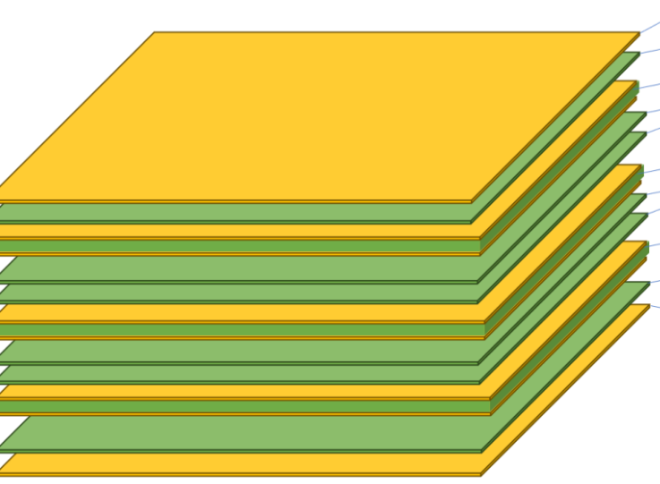
After feasibility approval, the next step is to rebuild the PCB stackup.
This is one of the most important stages of the entire layer-reduction process.
The revised stackup should clearly define:
- Core materials
- Prepreg materials
- Copper thickness
- Finished dielectric thickness
- Signal layers
- Ground layers
- Power layers
- Controlled-impedance structures
- Surface finish requirements
The goal should not be to remove layers indiscriminately. Instead, retain the functional electrical structure while eliminating only genuinely redundant layers.
Where practical, a symmetrical stackup should be considered to improve mechanical balance and reduce lamination-related warpage.
Preserve Critical Reference Planes
One of the most common mistakes is removing a ground layer simply because it contains little routing.
A ground layer may provide a critical reference for high-speed signals. Removing it can force return current to travel around discontinuities, increasing loop area and potentially increasing crosstalk, EMI, or impedance discontinuity.
Therefore, every removed layer should be evaluated in relation to the signals routed above and below it.
Recalculate Controlled Impedance
After changing the stackup, the original impedance calculation should not simply be reused.
The impedance of a transmission line depends on parameters such as:
- Trace width
- Copper thickness
- Dielectric thickness
- Dielectric constant
- Reference-plane geometry
- Trace-to-plane spacing
- Surface roughness
After layer reduction, the physical relationship between signal and reference layers may change significantly.
Critical 50 Ω, 90 Ω, 100 Ω, or other application-specific impedance structures should therefore be recalculated using the revised stackup and realistic manufacturing tolerances.
3. PCB Layout Optimization After Layer Reduction
Once the stackup has been finalized, the PCB layout must be updated accordingly.
Layer reduction normally reduces routing resources and may force previously separated signals onto the same layer. This makes routing discipline even more important.
High-speed, low-speed, RF, analog, and power circuits should be reviewed by functional region.
Engineers should pay particular attention to:
- High-speed differential pairs
- Clock traces
- RF transmission lines
- Sensitive analog signals
- Switching power loops
- High-current paths
- Connector transitions
- Via transitions
When signals change layers, the return path should also be considered. Ground stitching vias can sometimes help maintain return-current continuity around layer transitions, connectors, or RF structures.
The exact via arrangement should be determined according to the stackup, signal frequency, geometry, and EMC requirements rather than applying one universal spacing rule.
4. Rebuild the Power and Ground System
Reducing redundant power and ground layers can affect both current distribution and power integrity.
Before combining or removing power layers, engineers should identify:
- Continuous DC current paths
- Peak current paths
- High-frequency switching loops
- Ground return paths
- Decoupling capacitor locations
- Power-plane transitions
- Via current sharing
For high-current regions, trace width, copper thickness, plane area, and thermal conditions should be evaluated together.
For sensitive digital or RF circuits, power-distribution impedance and high-frequency return paths may be more important than simple DC resistance.
The revised design should therefore verify both power integrity and signal return-path continuity rather than focusing only on whether the circuit remains electrically connected.
5. SI/PI Simulation: Verify Performance After Layer Reduction
After layout optimization, SI/PI simulation should be performed for interfaces where layer reduction could affect electrical performance.
For high-speed interfaces, engineers can compare the original and revised designs using parameters such as:
- Differential impedance
- Single-ended impedance
- Eye diagram
- Insertion loss
- Return loss
- Crosstalk
- Overshoot and undershoot
- Timing margin
- Jitter
For power-distribution networks, analysis may include:
- DC voltage drop
- Current density
- PDN impedance
- Transient voltage deviation
- Power-plane resonance
- Decoupling effectiveness
The objective is not necessarily to prove that every numerical result is identical. Instead, the revised design should demonstrate sufficient performance margin against the product specification.
For lower-speed boards, full high-speed simulation may not be necessary. However, power paths, grounding, isolation, and potential coupling paths should still be reviewed.
6. EMC Review After Reducing Layers
Layer reduction can also change the electromagnetic behavior of a PCB.
Ground planes, reference planes, power planes, and signal-routing layers collectively determine the current-return structure. Removing a layer may increase loop area or create new coupling paths.
The EMC review should therefore examine:
- Reference-plane continuity
- High-speed return paths
- Power-loop area
- RF routing
- Ground stitching
- Connector interfaces
- Cable-entry regions
- Board-edge currents
- Potential common-mode current paths
Where necessary, engineers can use field simulation, near-field scanning, conducted-emission testing, or radiated-emission testing to verify the revised design.
7. DFM Review: Identify Manufacturing Risks Before Prototyping
A dedicated DFM review should be performed before the revised PCB enters production.
The review should cover at least four areas.
Stackup and Material Availability
Confirm that the revised core, prepreg, copper foil, and other materials are compatible with standard production.
Using commonly available materials can reduce procurement complexity, but the final choice must still meet electrical and reliability requirements.
Lamination Process
Check:
- Stackup symmetry
- Resin content
- Copper distribution
- Pressed dielectric thickness
- Resin flow
- Potential voids
- Delamination risk
- Board warpage
A thinner or asymmetric structure may require additional process control.
Hole and Via Manufacturing
Recalculate via aspect ratios after the board thickness changes.
Verify:
- Minimum hole diameter
- Finished hole tolerance
- Annular ring
- Hole-to-copper clearance
- Via-to-trace spacing
- Plating requirements
The revised design must remain within the manufacturer’s qualified process window.
Manufacturing Documentation
All revised information must be updated consistently, including:
- Stackup drawing
- Fabrication drawing
- PCB specifications
- Impedance requirements
- Material specifications
- Drill files
- Gerber or ODB++/IPC-2581 data
- Assembly documentation
- Engineering change records
This prevents the factory from accidentally using an outdated stackup or fabrication specification.
8. Prototype Validation: Compare the Original and Revised Boards
Prototype testing is essential because simulation cannot capture every manufacturing variable.
Where possible, engineers should compare the original and revised versions using equivalent test conditions.
Electrical Testing
Check:
- Controlled impedance
- High-speed interface performance
- Signal quality
- Power voltage drop
- Current-carrying performance
- Ground continuity
- RF performance where applicable
Mechanical and Assembly Testing
Evaluate:
- Finished board thickness
- Warpage
- Connector insertion and removal
- Screw fastening
- Enclosure assembly
- Component clearance
- Mechanical stress
Manufacturing Quality
Inspect:
- Copper thickness
- Dielectric thickness
- Plated-hole quality
- Solderability
- Solder-mask quality
- Lamination interfaces
- Surface finish
Cross-section analysis can be particularly useful for verifying whether the revised stackup has been manufactured as intended.
9. Reliability Validation and Production Qualification
If the PCB is used in demanding applications, reliability testing should reflect the actual product environment.
Depending on the application, testing may include:
- High- and low-temperature cycling
- High-temperature storage
- Humidity exposure
- Thermal shock
- Vibration
- Reflow simulation
- Solder-joint reliability testing
- Electrical insulation testing
The exact test temperature, humidity, cycle count, dwell time, and acceptance criteria should be defined by the product specification and applicable standards rather than treated as universal values.
If the revised board passes prototype validation, the project should proceed to a controlled pilot run before full-scale production.
During pilot production, monitor:
- First-pass yield
- Warpage distribution
- Impedance results
- Plated-hole quality
- Lamination defects
- Assembly yield
- Field-relevant functional tests
This creates a closed-loop transition from design verification to PCB manufacturing.
10. Establish a Controlled Engineering Change Process
Layer reduction should be treated as a formal engineering change rather than a simple CAD modification.
A complete change-control process can include:
Requirement review → feasibility assessment → stackup reconstruction → layout optimization → SI/PI analysis → EMC review → DFM review → prototype fabrication → electrical testing → reliability validation → pilot production → mass-production release
Each stage should have documented inputs, outputs, and approval criteria.
The original design should also be retained as a controlled reference so that electrical, mechanical, and manufacturing results can be compared objectively.
Conclusion
PCB layer reduction can reduce material consumption, simplify the board structure, and potentially lower manufacturing costs, but the process must be treated as a system-level engineering change.
Removing a layer can affect impedance, return paths, power distribution, EMC behavior, mechanical stiffness, lamination, and reliability. Therefore, the correct approach is not simply to delete an apparently unused layer, but to evaluate the entire electrical and physical structure before making the change.
A controlled workflow combining PCB stackup reconstruction, PCB design optimization, SI/PI simulation, DFM review, prototype testing, reliability validation, and production monitoring can significantly reduce the risk associated with layer reduction.
For projects requiring layer-count optimization, Kingda can support stackup evaluation, impedance analysis, DFM review, prototype validation, and PCB manufacturing, helping engineers balance cost reduction with electrical performance, manufacturability, and long-term PCB reliability.