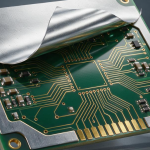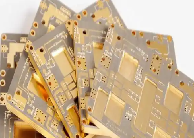
When converting a multilayer PCB from a non-standard finished thickness to a standard thickness, the key is to redesign the combination of PCB core and prepreg (PP) materials. Many engineers focus only on the final thickness value while overlooking resin flow, stackup symmetry, CTE compatibility, and lamination behavior. As a result, thickness changes can introduce PCB warpage, interlayer voids, dielectric-thickness variation, delamination, and other reliability risks.
Therefore, converting a non-standard multilayer PCB thickness to a standard specification is not simply an electrical or mechanical adjustment. It requires coordination between material selection, stackup design, lamination characteristics, impedance requirements, and manufacturing capability. Proper PCB stackup planning can improve production consistency while reducing unnecessary custom materials and manufacturing costs.
1. How Core and Prepreg Determine Multilayer PCB Thickness
A PCB core is a finished laminate with copper foil already bonded to both sides. Its thickness is relatively stable and it is normally treated as a predefined material during stackup design.
Prepreg (PP) consists primarily of glass fabric impregnated with resin. During lamination, the resin softens and flows under heat and pressure, filling the spaces between copper features and bonding adjacent layers. After curing, the compressed prepreg reaches a thickness that can differ from its nominal specification.
In practical multilayer PCB manufacturing, the finished board thickness can be considered as the combined contribution of:
- Core thickness
- Compressed prepreg thickness
- Copper foil thickness
- Surface copper and plating contributions, where applicable
However, prepreg should not be treated as a simple fixed-thickness material. Its final thickness depends on resin content, glass style, copper distribution, lamination pressure, temperature profile, and the amount of resin consumed during filling.
For this reason, engineers should use the PCB manufacturer’s validated post-lamination thickness data rather than simply adding the nominal PP thickness values.
For a non-standard board thickness, the required combination may involve special core specifications or an uncommon PP configuration. A standard thickness can often be achieved using commonly stocked materials and established lamination recipes. This can simplify procurement, shorten material preparation time, and improve process consistency.
2. Stackup Symmetry Should Be the First Priority
PCB stackup symmetry is one of the most important factors in controlling multilayer PCB warpage.
A non-standard board may originally use an asymmetric combination of cores, prepregs, and copper weights simply to reach a target thickness. If the material distribution above and below the board center is significantly different, the laminate can develop residual stress during heating and cooling.
During SMT reflow, additional thermal expansion and stress redistribution can further increase deformation. Excessive warpage may affect solder-paste printing, component placement, BGA soldering, and overall assembly yield.
A symmetrical stackup generally means that the material structure on both sides of the board’s central reference plane is balanced. Depending on the layer count, this may include corresponding:
- Core thicknesses
- Prepreg structures
- Copper weights
- Dielectric constructions
- Material systems
Symmetry does not necessarily mean that every electrical layer must perform the same function. Instead, the physical material distribution should be evaluated as a complete structure.
For 6-layer, 8-layer, and higher-layer-count boards, converting a non-standard thickness provides an opportunity to rebuild the stackup around a more balanced structure. Although this may require some layout and engineering changes, it can reduce lamination stress and improve production consistency.
3. Key Considerations When Matching Core and Prepreg
Use Compatible Material Systems
The PCB core and prepreg (PP) should generally be selected from compatible material systems. Resin chemistry, Tg, CTE, moisture behavior, and dielectric characteristics should be considered together.
Mixing unrelated laminate systems only to achieve a target thickness can introduce differences in thermal expansion and mechanical behavior. These differences may become more significant during lead-free reflow, thermal cycling, or other thermal stresses.
When a high-Tg laminate is required, the corresponding prepreg should be compatible with the selected resin system and lamination process.
Avoid Excessive Prepreg Layers
Using many thin PP sheets simply to achieve a particular board thickness is not always an efficient solution.
Every additional material interface introduces another process variable. Excessive resin-rich structures may also change resin flow behavior and affect dielectric uniformity.
Where the design and manufacturer process allow, engineers can evaluate whether a simpler PP construction can achieve the required dielectric thickness and bonding performance.
The objective is not simply to minimize the number of PP sheets, but to select a stable combination that matches the manufacturer’s lamination process.
Control Dielectric Thickness for Impedance
For high-speed designs, dielectric thickness is directly related to controlled impedance. The relationship also depends on trace geometry, copper thickness, dielectric constant, and the reference-plane configuration.
When an impedance-sensitive layer is involved, a stable core construction may offer more predictable dielectric thickness than a resin-rich prepreg structure. However, this is not a universal rule: properly characterized prepreg can also be used successfully when its pressed thickness is controlled.
Therefore, the correct approach is to obtain the manufacturer’s actual pressed dielectric thickness data and use it for impedance control calculations.
This is particularly important for high-speed differential pairs, RF traces, and other transmission lines where small changes in geometry can affect impedance and signal integrity.
Keep Copper Thickness Consistent
Copper thickness should not be changed casually simply to make the total board thickness reach a target value.
Changing outer- or inner-layer copper affects more than finished thickness. It can also influence:
- Trace resistance
- Controlled impedance
- Current-carrying capability
- Copper balance
- Thermal performance
- Etching requirements
- Manufacturing tolerances
For high-current power layers, copper thickness should be selected according to the required electrical and thermal performance rather than used as a convenient thickness adjustment.
4. Predicting Thickness Variation During Lamination
Even when standard cores and PP materials are used, the final board thickness will have manufacturing tolerance.
The actual compressed thickness of prepreg depends on its construction and resin content, as well as the amount of resin consumed by surrounding copper patterns.
For example, a nominal PP thickness should not automatically be treated as its final dielectric thickness after lamination. The actual pressed value must be established through the manufacturer’s material data and process characterization.
During PCB manufacturing, engineers should therefore avoid designing the target thickness directly at the extreme edge of the acceptable tolerance range.
A better approach is to:
- Define the target finished thickness and tolerance.
- Select available core and PP combinations.
- Obtain validated pressed-thickness data from the PCB manufacturer.
- Recalculate the complete stackup.
- Check impedance and dielectric thickness.
- Review copper distribution and warpage risk.
- Confirm the proposed structure through prototype or qualification builds where necessary.
5. Copper Balance and Warpage Control
Material symmetry alone does not guarantee low warpage.
Copper distribution also plays an important role because copper and laminate materials have different thermal expansion characteristics. A board with heavy copper concentration on one side and relatively little copper on the other may experience uneven thermal behavior during lamination and assembly.
For this reason, copper balance should be evaluated across the entire board.
Large copper areas can sometimes be balanced with appropriately designed copper features on the opposite side, provided that electrical isolation, thermal requirements, signal integrity, and manufacturing rules are maintained.
For power and ground planes, engineers should consider both electrical functionality and physical copper distribution rather than optimizing only one factor.
6. Recalculate Via and Manufacturing Constraints After Thickness Changes
Changing the finished thickness also changes the relationship between hole diameter and board thickness.
The PCB manufacturing team should therefore recheck via aspect ratio, plating capability, drill size, annular ring, and registration requirements after the stackup is modified.
A thicker finished board combined with very small through-holes can increase the difficulty of reliable hole plating. Blind and buried vias also require their own process-capability evaluation.
The stackup change should therefore be reviewed together with:
- Drill diameter
- Via aspect ratio
- Copper plating requirements
- Layer-to-layer registration
- Lamination capability
- Final thickness tolerance
- Surface finish requirements
This prevents a seemingly simple thickness adjustment from creating a new manufacturing bottleneck.
7. Multilayer PCB Non-Standard-to-Standard Thickness Review Checklist
Before converting a non-standard multilayer PCB to a standard thickness, engineers should verify the following:
- Is the PCB stackup physically balanced and sufficiently symmetrical?
- Are the selected core and prepreg (PP) materials compatible?
- Are Tg, CTE, resin system, and moisture characteristics appropriate for the application?
- Has the actual pressed PP thickness been confirmed?
- Has impedance control been recalculated using the actual dielectric construction?
- Is copper distribution balanced across the board?
- Has the required copper thickness for power circuits been preserved?
- Has via aspect ratio been recalculated?
- Are drilling, plating, registration, and lamination capabilities compatible with the revised structure?
- Has warpage risk been evaluated for both PCB fabrication and SMT assembly?
- Does the revised stackup require prototype or reliability validation?
Conclusion
Converting a non-standard multilayer PCB thickness to a standard specification should not be treated as simply changing one thickness number. The combination of PCB core, prepreg (PP), copper thickness, dielectric construction, stackup symmetry, and lamination behavior determines whether the revised design can be manufactured consistently.
A well-designed PCB stackup should balance electrical performance, mechanical stability, thermal behavior, impedance control, and manufacturing capability. By using validated pressed-material data, controlling copper balance, maintaining compatible material systems, and reassessing vias and lamination requirements, engineers can reduce the risk of warpage, delamination, voids, and impedance variation during mass production.
Kingda can support multilayer PCB stackup evaluation, material selection, DFM review, impedance analysis, and manufacturing validation to help engineers convert non-standard board structures into practical, production-ready designs.