Different PCB packaging materials can provide very different levels of protection, even when they are used for the same PCB product. When packaging is evaluated only from a cost perspective, important material characteristics may be overlooked, resulting in ESD exposure, surface scratches, board deformation, damaged corners, moisture ingress, or package failure during transportation.
A complete packaging system normally consists of four functional categories: materials that directly contact the PCB, cushioning materials, sealing and shielding materials, and external reinforcement materials.
The correct combination should be selected according to PCB structure, surface finish, mechanical sensitivity, ESD requirements, transportation conditions, storage duration, and product reliability requirements.
1. Selecting Materials That Directly Contact the PCB
Materials that directly contact the PCB surface include separator sheets, foam, and thermoformed trays. Because these materials may contact solder mask, pads, copper surfaces, or gold fingers, their cleanliness, surface characteristics, and ESD performance require careful evaluation.
ESD-safe separator paper can be used to prevent direct contact between adjacent boards. For sensitive surface finishes, the separator should also be evaluated for sulfur, ionic contamination, particles, and other substances that could affect the PCB surface.
The separator should provide sufficient coverage without creating excessive pressure on board edges or sensitive features. For irregularly shaped boards or products with exposed gold fingers, customized trays can provide more consistent positioning and reduce board-to-board movement.
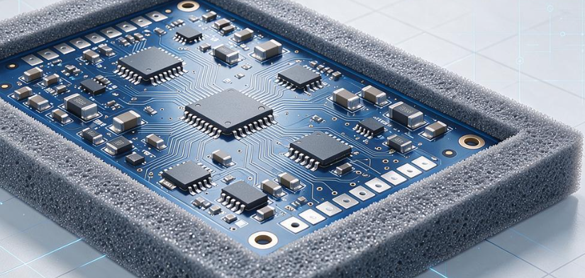
Foam selection should consider both cushioning performance and material stability. EPE and EVA are common polymer foam options, but their actual suitability depends on density, compression characteristics, surface cleanliness, ESD performance, and the transportation environment.
For high-reliability applications, packaging engineers should avoid selecting foam solely according to price or softness. The material should be validated for compression set, particle generation, moisture behavior, and compatibility with the PCB surface.
Common mistakes to avoid:
- Ordinary newspaper directly contacting PCB surfaces
- Non-ESD-safe foam used around sensitive products
- Materials with excessive particle generation
- Materials with unknown chemical compatibility
- Separators that are too small to protect the entire board
- Excessively soft cushioning that collapses under long-term compression
The objective of PCB packaging materials selection is not simply to separate boards. The materials must protect the PCB without introducing contamination, static-electricity, abrasion, or mechanical stress.
2. Choosing ESD-Shielding and Moisture-Barrier Bags
Not all antistatic bags provide the same level of protection.
Dissipative or antistatic bags can reduce charge accumulation on the packaging surface, but they do not necessarily provide effective shielding against external electrostatic fields. When a product requires protection from external electrostatic discharge or field exposure, a properly specified shielding bag should be considered.
Metalized ESD shielding bags can provide electromagnetic and electrostatic shielding when correctly constructed and sealed. Their performance depends on the packaging structure, shielding layer, seams, closure method, and handling conditions.
For products requiring moisture protection, a moisture-barrier bag may be combined with desiccant and a humidity indicator. Aluminum-laminated barrier packaging can provide stronger moisture protection than a basic antistatic bag, but the appropriate material should be selected according to the PCB’s storage and transportation requirements.
Packaging integrity is equally important. Sharp PCB corners can puncture thin films and compromise the entire packaging system. Protective corner pieces or appropriately designed separators can reduce this risk.
The sealing method should also be compatible with ESD and moisture-control requirements. Ordinary adhesive tape should not automatically be assumed to provide ESD-safe performance. Where electrostatic-sensitive products are involved, the complete packaging and handling system should be evaluated.
3. Selecting Cushioning and Compression-Protection Materials
Cushioning materials protect PCBs from vibration, impact, compression, and movement during transportation.
A common packaging failure occurs when excessive empty space remains inside the carton. During vehicle transportation or handling, the PCB stack can move repeatedly and collide with the carton or other packaging components.
However, eliminating empty space does not mean tightly compressing the PCB stack. The packaging system should provide sufficient restraint while avoiding excessive mechanical loading.
Cushioning materials should therefore be evaluated for:
- Compression strength
- Compression set
- Shock absorption
- Vibration damping
- Recovery characteristics
- Particle generation
- ESD performance
- Moisture behavior
External cartons also play an important role in PCB mechanical protection.
The required carton construction depends on package size, total weight, stacking conditions, transportation distance, and expected handling environment. Single-wall or double-wall corrugated cartons may be appropriate for different logistics conditions, but the selection should be based on actual package requirements rather than a universal rule.
For larger or heavier PCB shipments, stronger corrugated structures and internal reinforcement may be necessary to prevent carton deformation.
Corner protection can further improve package strength, particularly when the carton is exposed to stacking or impact during transportation.
4. Packaging Combinations for Different PCB Applications
There is no single packaging configuration suitable for every PCB.
A general selection framework can be structured as follows:
| PCB application | Recommended packaging approach |
|---|---|
| Standard consumer PCB | ESD protection + separator + suitable corrugated carton |
| Industrial multilayer PCB | Shielding bag + ESD-safe separator/cushion + reinforced carton |
| Thin or HDI PCB | Moisture barrier where required + ESD-safe separator + structural support |
| Gold-finger PCB | Individual separation or tray + contact-area protection + reinforced packaging |
| High-frequency PCB | Surface protection + ESD control + contamination and moisture management |
| Large PCB panel | Rigid support + cushioning + reinforced outer carton |
| High-reliability PCB | Validated ESD, moisture, mechanical, and traceability controls |
For thin PCBs and HDI boards, the packaging system should place greater emphasis on bending and compression control. For gold-finger products, abrasion and contamination of the contact surface are critical considerations.
For high-frequency or precision PCBs, surface contamination and moisture exposure may require additional control depending on the material system and application.
5. How to Balance Protection Level and Packaging Cost
Choosing the highest-grade material for every PCB is not necessarily the most efficient approach. At the same time, reducing packaging cost by removing essential protection can create much higher downstream losses.
A practical PCB packaging decision should consider:
- PCB thickness and mechanical rigidity
- Board dimensions and panel structure
- Surface finish and exposed contact areas
- ESD sensitivity
- Moisture sensitivity
- Transportation distance
- Transportation mode
- Expected storage duration
- Package stacking conditions
- Customer unpacking and handling procedures
For example, a standard rigid FR-4 board shipped locally may require a significantly different packaging system from a thin HDI board transported overseas for several weeks.
The packaging specification should therefore be matched to the actual risk profile rather than determined only by PCB quantity or unit packaging cost.
6. IQC and Incoming Control of Packaging Materials
Packaging materials should also be subject to incoming quality control.
Depending on the material type, IQC may evaluate:
- Surface resistance or electrical properties for ESD materials
- Bag sealing and barrier integrity
- Material thickness
- Dimensional accuracy
- Foam density and compression characteristics
- Particle or surface cleanliness
- Material identification and traceability
- Packaging supplier certificates where applicable
For ESD-sensitive packaging, electrical resistance measurements should be performed using an appropriate test method and acceptance specification rather than relying only on the supplier’s label.
For moisture-barrier bags, seal integrity and barrier performance should be verified according to the packaging specification.
A rejected packaging material should not enter the packing workstation simply because the PCB itself has passed inspection. Packaging is part of the product-protection system and should therefore be included in the overall PCB quality control process.
7. Packaging Validation Before Mass Production
For new PCB products or significant packaging changes, a packaging validation process can help identify hidden risks before mass shipment.
Validation may include:
Packaging Assembly → Compression Assessment → Vibration Testing → Shock/Drop Evaluation → ESD Verification → Moisture Protection Check → Visual Inspection → Customer Unpacking Evaluation
The exact tests should be selected according to product requirements and transportation conditions.
For thin boards, deformation should be evaluated after packaging and transportation simulation. For gold-finger products, the contact areas should be inspected for scratches or contamination.
For moisture-sensitive products, packaging integrity should be verified together with the storage period and environmental exposure requirements.
This approach allows PCB packaging materials to be evaluated as an integrated protection system rather than as isolated components.
8. Kingda’s PCB Packaging Approach
Specialized PCBs should not simply use a standard packaging template designed for conventional boards.
Kingda can support packaging solutions based on PCB thickness, dimensions, structure, surface finish, ESD requirements, mechanical sensitivity, transportation conditions, and storage requirements.
By combining appropriate ESD protection, cushioning, separators, moisture barriers, structural supports, and external reinforcement, packaging can be integrated into the PCB quality-control process from final inspection through delivery.
The right packaging strategy should achieve a practical balance between protection, logistics efficiency, material cost, and product reliability.
For thin, HDI, gold-finger, large-panel, high-frequency, and other sensitive PCBs, selecting the right PCB packaging materials can significantly reduce the risk of transportation-related damage and help maintain product quality until the boards reach the customer’s production line.