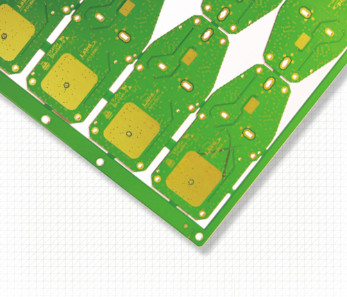
Standard 1.6 mm FR-4 PCBs generally have sufficient mechanical rigidity to tolerate conventional packaging and transportation conditions. However, thin PCB packaging requires a different approach when boards are 0.4–0.8 mm thick or have other mechanically sensitive structures.
HDI boards, large-format panels, gold-finger PCBs, and thick-copper boards may also require specialized packaging because their structural characteristics and surface features create different transportation risks.
Inadequate packaging can expose PCBs to electrostatic discharge (ESD), bending, compression, vibration, abrasion, moisture, and contamination. These risks may not be visible immediately but can contribute to assembly problems or electrical failures later.
A suitable PCB packaging strategy should therefore be designed according to board thickness, dimensions, stackup, surface finish, panel structure, transportation conditions, and customer handling requirements.
1. Key Packaging Risks for Thin PCBs and HDI Boards
PCBs below approximately 0.8 mm can have significantly lower mechanical rigidity than standard boards. Excessive stacking pressure or uneven support may cause bending or warpage.
If deformation exceeds the assembly process capability, downstream SMT operations may experience placement instability, poor solder-joint formation, or difficulty maintaining coplanarity.
Thin PCBs also require protection against edge and corner damage. Routed edges or sharp corners can puncture protective bags or separators, potentially compromising ESD or moisture protection.
HDI boards introduce additional considerations. Their fine lines, microvias, and thin dielectric structures require careful handling. Mechanical damage that appears minor on the surface may still affect electrical performance or reliability.
Gold-finger PCBs require special attention because the plated contact areas are functional interfaces. Scratches, dents, or contamination on the gold fingers can increase contact resistance or interfere with connector engagement.
Large PCB panels also have greater sensitivity to bending because their overall dimensions can increase the mechanical leverage during transportation. Areas containing V-cut or other depanelization features can become local stress-concentration points.
For these products, ESD protection for PCBs and mechanical protection should be considered together rather than as two independent packaging requirements.
2. ESD Protection and Layered Separation
Thin boards should not automatically be stacked in large quantities. The allowable stack height should be determined through mechanical testing and packaging validation.
A practical separation system may include ESD-safe, non-contaminating separator sheets between boards. The separator should provide sufficient coverage so that adjacent PCB surfaces and edges do not directly contact each other.
For highly sensitive thin boards, individual or small-batch placement in an ESD-safe tray can provide better mechanical support. A tray with dedicated pockets can prevent direct compression between PCB surfaces and reduce sliding during transportation.
When custom trays are not practical, a properly selected ESD-safe foam or rigid separator can distribute the load across a larger area. Ordinary soft packaging foam should not be assumed to provide adequate protection because it may compress permanently during long-term stacking or transportation.
For HDI products, HDI PCB packaging should provide appropriate ESD shielding, mechanical separation, and environmental protection. The packaging material should be selected according to the customer’s ESD requirements and the sensitivity of the product.
ESD shielding bags can be used when shielding from external electrostatic fields is required. However, simply using an antistatic bag does not guarantee complete ESD protection. The entire packaging system—including separators, trays, bags, handling equipment, and grounding practices—should be evaluated as a system.
3. Avoiding Compression and Deformation During Packaging
Mechanical protection should prevent concentrated loads from being transferred directly to sensitive PCB surfaces.
For thin boards, rigid or semi-rigid support plates can be placed above and below a stack to distribute compression. The support structure should be sufficiently rigid and appropriately sized for the PCB dimensions.
Packaging should also minimize free movement inside the carton. Excessive movement allows boards to collide, slide, or experience repeated bending during transportation.
For large panels, support points should be designed around the actual panel geometry. V-cut locations and narrow connecting sections should not become unintended load-bearing points.
If vacuum packaging is used, the packaging process should be validated for the specific PCB construction. Excessive external pressure during vacuum packaging may deform mechanically sensitive boards if the support structure is inadequate.
The goal is to achieve reliable sealing and environmental protection without creating a new mechanical risk.
4. Special Protection for Gold-Finger PCBs and Large Panels
Gold-finger areas should be isolated from direct contact with other boards and packaging surfaces that could scratch or contaminate the plated contacts.
Where appropriate, protective film or dedicated separators can be used to prevent abrasion during handling and transportation. Gold fingers should also be positioned so that they do not become concentrated load points when multiple boards are stacked.
During unpacking and inspection, operators should avoid touching contact surfaces directly. ESD-safe handling procedures, gloves where appropriate, and controlled workstations can help reduce contamination and electrostatic risks.
For large panels, hard ESD-safe separator plates can be used above and below the panel stack. The objective is to distribute mechanical loads and prevent localized stress around V-cut or routing features.
The shipping carton should also provide sufficient structural strength for the package size and total load. Internal voids should be minimized so that panels cannot move freely during transportation.
5. Warehouse and Logistics Controls
Packaging protection can be compromised if warehouse and logistics practices are not controlled.
The maximum package weight should be determined according to the board construction, packaging design, manual-handling requirements, and carton strength. A fixed universal weight limit should not be applied to every PCB product.
Similarly, carton stacking height should be validated according to package compression strength and storage conditions. Sensitive thin-board packages should not be placed beneath heavy materials.
Clear handling labels can identify packages that require special treatment, such as:
- Thin PCB — Handle With Care
- ESD Sensitive
- Do Not Stack Heavy Loads
- Keep Dry
- Protect Gold-Finger Area
- Avoid Excessive Bending
For long-distance transportation, vibration, shock, humidity, temperature cycling, and package compression may need to be considered during packaging validation.
This is especially important for thin PCB packaging because a package that appears adequate during warehouse storage may behave differently under repeated transportation vibration.
6. Incoming Inspection After Transportation
The customer should inspect the external package before opening it. Visible carton deformation, crushing, water damage, broken seals, or other abnormal conditions should be recorded.
After opening, thin PCBs can be checked for:
- Board warpage
- Edge or corner damage
- Surface scratches
- Copper or gold-finger damage
- Contamination
- Delamination or blistering
- Packaging integrity
- Moisture-indicator status where applicable
For HDI products, additional inspection may be appropriate depending on the product specification and reliability requirements.
A damaged package does not automatically mean that every PCB inside is defective, but it should trigger an appropriate inspection and risk assessment before production release.
If significant deformation is observed, boards should not be sent directly into SMT production without confirming that they remain within the applicable assembly requirements.
7. Designing Packaging According to PCB Structure
There is no single PCB packaging method suitable for every PCB type.
Packaging design should consider at least the following factors:
| PCB characteristic | Main packaging consideration |
|---|---|
| Thin PCB | Bending and compression protection |
| HDI PCB | ESD, surface, and mechanical protection |
| Gold-finger PCB | Contact-area protection and contamination control |
| Large panel | Bending, vibration, and V-cut stress |
| Thick-copper PCB | Weight and mechanical support |
| Fine-line PCB | Surface protection and abrasion prevention |
| High-reliability PCB | Moisture, ESD, and traceability control |
Packaging should also be evaluated together with the customer’s unpacking process. A package that protects the board during shipping but causes excessive handling stress during opening is not an optimized solution.
8. Kingda’s Approach to Special PCB Packaging
Special-structure PCBs should not simply use the same packaging template designed for standard FR-4 boards.
Kingda can support customized PCB packaging strategies for thin PCBs, HDI boards, large panels, gold-finger boards, thick-copper PCBs, and other mechanically or electrostatically sensitive products.
By considering board geometry, thickness, surface finish, ESD requirements, mechanical loading, transportation conditions, and customer handling procedures, packaging can be designed as part of the overall manufacturing quality system.
The objective is not simply to prevent visible shipping damage. Effective packaging should maintain PCB integrity from final inspection through storage, transportation, customer unpacking, and SMT assembly.
For sensitive products, ESD protection for PCBs and mechanical protection should therefore be validated together with the manufacturing and quality-control process.