After PCB fabrication, inspection, and testing are completed, packaging becomes an important part of protecting board quality during shipment and storage. Problems such as electrostatic exposure, board-edge damage, surface scratches, warpage, moisture absorption, and compression damage may not originate from the manufacturing process itself. They can also occur during handling, packaging, transportation, or storage.
IPC-1601 provides guidelines for printed board handling, packaging, environmental conditions, and storage. Its purpose is to help protect printed boards from contamination, physical damage, solderability degradation, ESD when necessary, and moisture uptake. IPC also notes that moisture absorbed by laminate can expand during soldering and may contribute to delamination or excessive stress on plated-hole structures.
For this reason, PCB packaging should be treated as part of the overall quality-control system rather than simply as the final step of shipping.
1. Understanding the Main PCB Packaging Failure Risks
Packaging-related PCB failures generally fall into several categories, including ESD exposure, mechanical damage, moisture-related degradation, contamination, and surface damage.
ESD-related damage can be immediately detectable or difficult to identify. A severe electrical event may produce an obvious failure, while a less obvious event may cause damage that is not detected during routine inspection.
For products containing sensitive electronic devices, ESD protection should be designed according to the actual sensitivity of the product and the requirements of the applicable ESD control program. Packaging requirements for electrostatic-discharge-sensitive items are specifically addressed by ANSI/ESD S541.
Mechanical damage can include:
- Cracked or chipped board edges
- Damage around V-cut or routing features
- Surface scratches or pressure marks
- Gold-finger damage
- PCB warpage
- Localized compression
- Board-to-board abrasion
- Damage caused by excessive vibration
Thin PCBs, HDI boards, large-format panels, and other mechanically sensitive structures generally require more carefully designed support than standard rigid boards.
Some mechanical defects are immediately visible, while internal damage may require additional inspection or reliability testing to identify. Packaging should therefore be designed to prevent excessive mechanical loading rather than relying only on final visual inspection.
2. IPC-1601 and the Role of PCB Packaging
A common misunderstanding is that IPC-1601 defines one mandatory packaging configuration for every PCB.
In practice, IPC-1601 is a guideline covering handling, packaging materials and methods, environmental conditions, and storage. It is intended to be used together with applicable customer, product, assembly, material, and other industry requirements.
This distinction is important when developing a packaging specification.
Instead of writing a requirement such as “all PCBs must use the same bag, stack height, and carton weight,” engineers should define packaging according to:
- PCB thickness
- Board dimensions
- Panel structure
- Surface finish
- Mechanical sensitivity
- ESD sensitivity
- Moisture sensitivity
- Transportation method
- Transportation duration
- Storage conditions
- Customer handling requirements
This approach makes PCB packaging more closely aligned with actual product risk.
3. ESD Packaging: Dissipative Materials vs. Shielding Packaging
ESD protection is another area where packaging terminology is frequently misunderstood.
Dissipative materials are designed to control charge dissipation, but a dissipative package is not automatically equivalent to a shielding package. The EOS/ESD Association explains that packaging for ESDS items may need properties including low charging, charge dissipation, and discharge shielding depending on where and how the item is handled.
ANSI/ESD S541 specifically addresses packaging materials used to protect electrostatic-discharge-sensitive items during production, transportation, and storage.
Therefore, engineers should distinguish among:
- Antistatic or low-charging materials
- Dissipative materials
- Conductive materials
- ESD shielding materials
- Moisture-barrier packaging
The appropriate combination depends on the ESD control program and product sensitivity.
A pink antistatic bag, for example, should not automatically be treated as a substitute for a shielding bag when external electrostatic-field protection is required.
Packaging should also be evaluated as a complete system. The bag, separator, foam, tray, carton, handling process, and grounding practices all contribute to the final protection level.
4. Moisture Protection and Dry Packaging
Moisture is another important consideration in PCB storage and transportation.
IPC-1601 identifies moisture uptake as a potential risk because absorbed moisture can expand during soldering and may contribute to internal delamination or stress on plated structures.
For products requiring dry packaging, a typical system may include:
Moisture Barrier Bag (MBB) + Desiccant + Humidity Indicator Card (HIC)
IPC describes dry packaging in this general configuration and defines the role of MBB, HIC, and water-vapor transmission characteristics.
IPC technical guidance also recommends selecting packaging materials that adequately protect the PCB during shipment and storage and using moisture-barrier packaging, desiccant, and humidity indicators where required.
The packaging specification should therefore consider the PCB material system, storage duration, environmental exposure, assembly process, and customer requirements rather than automatically applying one moisture-control method to every board.
5. Mechanical Protection and PCB Stacking
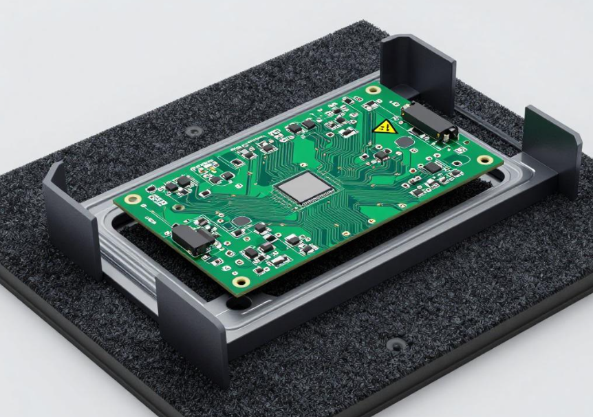
Mechanical protection should prevent direct board-to-board contact, excessive compression, impact, and uncontrolled movement.
Separators can be used between boards to reduce surface abrasion and distribute mechanical loads. For thin or mechanically sensitive PCBs, rigid or semi-rigid support structures may be required.
The number of PCBs allowed in one stack should not be defined only by a universal quantity such as 20 pieces. It should be determined according to board thickness, dimensions, stiffness, surface structure, separator characteristics, package design, and transportation conditions.
Large panels require particular attention to stress concentration. V-cut, routing channels, narrow connecting areas, and other structural features may have lower mechanical strength than the surrounding PCB.
The packaging design should prevent these areas from becoming concentrated load points.
A practical PCB mechanical protection strategy may include:
PCB Separation → Load Distribution → Edge Protection → Rigid Support → Cushioning → Carton Reinforcement
This layered approach is generally more reliable than relying on a single foam layer or external carton.
6. Outer Carton and Transportation Protection
The outer carton protects the entire packaging system from compression, impact, vibration, and handling damage.
Carton selection should consider:
- Total package weight
- Package dimensions
- Stacking conditions
- Transportation distance
- Transportation mode
- Expected vibration and impact
- Storage environment
- Required package strength
Double-wall corrugated cartons may be appropriate for heavier or more demanding shipments, but the correct carton grade should be determined from the actual package design and logistics conditions.
Likewise, a fixed maximum carton weight or universal stacking limit should not be presented as an IPC-1601 requirement unless the specific requirement is actually documented in the applicable revision or customer specification.
Internal voids should be controlled so that PCB stacks cannot move excessively during transportation. At the same time, cushioning should not create excessive compression.
Handling labels such as Fragile, ESD Sensitive, Keep Dry, or Do Not Stack can supplement the packaging design, but labels should never be considered a substitute for adequate mechanical protection.
7. Common Misapplications of PCB Packaging Requirements
Several packaging mistakes frequently occur when standards are applied too literally or incompletely.
Mistake 1: Using only an antistatic outer bag
An outer bag cannot compensate for unsuitable materials that directly contact the PCB. The complete packaging system must provide the required ESD properties.
Mistake 2: Focusing on ESD while ignoring mechanical protection
A shielding bag may provide appropriate ESD protection while doing nothing to prevent compression, bending, or abrasion. ESD and mechanical protection must therefore be evaluated separately and then integrated.
Mistake 3: Applying one packaging configuration to every PCB
A 1.6 mm rigid FR-4 board and a thin HDI panel do not necessarily have the same mechanical or moisture risks. Packaging should be matched to the actual PCB construction.
Mistake 4: Treating IPC-1601 as the only applicable requirement
IPC-1601 provides handling and storage guidance, but other requirements may apply depending on the product and application. ESD packaging may involve ANSI/ESD S541, while an overall ESD control program is addressed by ANSI/ESD S20.20.
Mistake 5: Specifying packaging without validation
A packaging design that looks appropriate on paper may still fail under vibration, compression, humidity, or repeated handling. Packaging validation should therefore reflect the actual transportation and storage environment.
8. Establishing a Complete PCB Packaging Control Process
A professional PCB packaging process can be organized into the following workflow:
Product Risk Assessment → Packaging Material Selection → ESD Evaluation → Moisture Protection Review → Mechanical Protection Design → Packaging Assembly → Transportation Validation → Incoming Inspection → Storage Control → Traceability
Packaging specifications should also be documented and controlled. Changes to bags, separators, foam, trays, cartons, sealing methods, or package configuration should be reviewed before mass implementation.
For sensitive PCBs, the packaging specification can include:
- Approved packaging materials
- ESD requirements
- Moisture-barrier requirements
- Separator specifications
- Maximum stack configuration
- Edge and corner protection
- Carton specifications
- Storage conditions
- Handling instructions
- Inspection requirements
- Packaging traceability
This creates a closed-loop PCB quality control system that connects manufacturing, packaging, logistics, and customer handling.
9. Kingda’s Approach to PCB Packaging
PCB packaging is not simply a matter of placing finished boards into bags and cartons. It is a protection system designed to maintain PCB condition throughout handling, storage, transportation, and customer unpacking.
Kingda can develop PCB packaging solutions based on PCB thickness, board structure, surface finish, ESD sensitivity, moisture requirements, transportation conditions, and storage duration.
For thin PCBs, HDI boards, gold-finger boards, large panels, and other sensitive products, the packaging design can combine ESD shielding, moisture protection, board separation, cushioning, edge protection, and carton reinforcement.
The objective is to preserve PCB quality after final inspection and prevent packaging-related risks from becoming customer-side production problems.
By integrating IPC-1601 guidance with applicable ESD, moisture-control, customer, and product requirements, manufacturers can establish a packaging process that is both technically appropriate and traceable.