14-Layer PCB Stackup: PCB Design, PCB Manufacturing & High-Speed PCB Design Guide
As electronic products continue to become smaller, faster, and more functionally integrated, multilayer printed circuit boards (PCBs) are increasingly important in modern electronics. A 14-layer PCB provides significantly more routing resources than conventional 4-layer or 6-layer boards, making it suitable for complex systems that require high component density, controlled impedance, power distribution, and reliable signal integrity.
A well-designed 14-layer stackup can support applications such as automotive electronics, industrial control systems, telecommunications equipment, servers, medical electronics, aerospace systems, and other high-density electronic products. Depending on the application, a 14-layer board can be manufactured as a rigid PCB, rigid-flex PCB, or other customized multilayer configuration.
For engineers preparing a multilayer board for production, understanding the 14-layer PCB stackup is essential. The stackup determines how signal layers, power planes, ground planes, dielectric materials, and copper layers are arranged. It directly influences impedance, crosstalk, electromagnetic compatibility (EMC), thermal performance, manufacturability, and overall PCB reliability.
What Is a 14-Layer PCB Stackup?
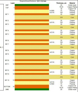
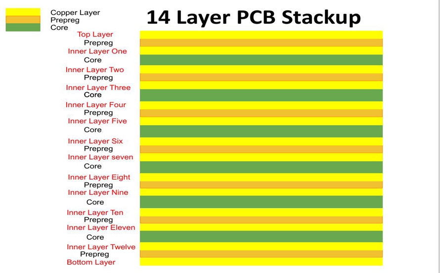
A 14-layer PCB stackup is the predefined arrangement of 14 conductive copper layers separated by dielectric materials such as core laminates and prepreg.
A typical 14-layer PCB may contain:
- High-speed signal layers
- Low-speed signal layers
- Power planes
- Ground planes
- Core materials
- Prepreg dielectric layers
- Solder mask on the outer surfaces
The exact layer arrangement depends on the electrical and mechanical requirements of the product.
For example, a high-speed 14-layer PCB may dedicate several internal layers to solid ground and power planes while placing high-speed signals adjacent to reference planes. This arrangement helps provide controlled return paths and improves electromagnetic performance.
Fourteen-layer boards are particularly useful when a design requires more routing capacity than an 8-layer or 10-layer PCB can provide. Instead of increasing the physical size of the board, engineers can add internal layers to accommodate additional signals, power distribution, and ground structures.
This is especially valuable in applications where PCB space is limited but circuit complexity is high.
Why Use a 14-Layer PCB?
The main reason to use a 14-layer PCB is to increase circuit density while maintaining manageable board dimensions.
A multilayer structure can provide several important advantages:
- Higher routing density
- Better power distribution
- Dedicated ground planes
- Improved signal integrity
- Controlled impedance
- Reduced crosstalk
- Better EMI/EMC performance
- More efficient thermal management
- Greater flexibility for component placement
- Improved electrical isolation between different circuit functions
For example, automotive electronic control units (ECUs), industrial controllers, communication equipment, and high-performance computing hardware may contain a large number of high-speed interfaces and power circuits. A 14-layer structure provides additional internal routing and reference-plane resources without requiring an excessively large PCB footprint.
Key Factors in 14-Layer PCB Stackup Design
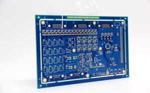
Before starting PCB Design, engineers should define the electrical, mechanical, thermal, and manufacturing requirements of the board.
1. PCB Electrical Requirements
The first consideration is the electrical architecture of the PCB.
A 14-layer stackup may need to support:
- High-speed digital signals
- Differential pairs
- RF signals
- Power distribution
- Analog circuits
- Sensitive clock signals
- High-current circuits
- Controlled-impedance transmission lines
High-speed signal layers should have a well-defined reference plane. A signal layer positioned close to a solid ground plane can provide a more predictable return-current path and reduce unwanted electromagnetic radiation.
For controlled-impedance designs, the dielectric thickness, dielectric constant (Dk), copper thickness, trace width, and trace-to-plane spacing must be considered together.
2. Copper Thickness
Copper thickness has a direct influence on current capacity, resistance, thermal performance, impedance, and manufacturing cost.
Outer-layer copper may be different from inner-layer copper because the outer layers are often processed differently during PCB fabrication.
Instead of applying one fixed copper thickness to all 14 layers, engineers should select copper weights according to the requirements of each layer.
For example:
- Signal layers may use relatively thin copper.
- Power layers may require heavier copper.
- High-current paths may require wider traces, copper pours, or dedicated power planes.
- Fine-pitch BGA routing may benefit from controlled copper thickness and appropriate manufacturing tolerances.
The final copper thickness should be confirmed with the PCB manufacturer before fabrication.
3. Dielectric Thickness
Dielectric thickness is one of the most important variables in a 14-layer stackup.
It affects:
- Controlled impedance
- Crosstalk
- Signal propagation
- Capacitance between layers
- Electrical spacing
- Mechanical thickness
- Manufacturing feasibility
For high-speed PCB design, signal layers should generally be positioned close enough to their reference planes to provide a predictable electromagnetic environment.
However, there is no universal dielectric thickness that works for every 14-layer PCB. The actual value should be calculated according to the selected laminate system, copper thickness, trace geometry, target impedance, and manufacturer capabilities.
4. Material Selection
The material system must match the application’s electrical, thermal, and reliability requirements.
FR-4 remains widely used for many 14-layer PCBs because of its cost-effectiveness and mature manufacturing process. However, high-speed or RF applications may require low-loss laminates with better Dk/Df characteristics and tighter electrical consistency.
Important material parameters include:
- Dielectric constant (Dk)
- Dissipation factor (Df)
- Glass transition temperature (Tg)
- Decomposition temperature (Td)
- Coefficient of thermal expansion (CTE)
- Thermal conductivity
- Moisture resistance
- Dimensional stability
For demanding applications, engineers should use the manufacturer’s actual laminate data rather than relying only on generic material values.
Main Components of a 14-Layer PCB Stackup
A typical multilayer PCB consists of copper layers separated by dielectric materials.
Copper Layers
The 14 conductive layers can be assigned as:
- High-speed signal layers
- General signal layers
- Ground planes
- Power planes
- Mixed power/signal layers where appropriate
A common strategy is to dedicate several internal layers to ground and power distribution while reserving other layers for signal routing.
The exact assignment depends on the circuit architecture.
Prepreg
Prepreg is a resin-and-glass-fiber dielectric material used to bond copper layers together during lamination.
During the lamination process, heat and pressure cause the resin to flow and cure, forming a stable multilayer structure.
Prepreg selection influences:
- Dielectric thickness
- Impedance
- Resin content
- Lamination behavior
- Mechanical stability
- Electrical performance
The final dielectric thickness after lamination must be considered rather than simply using the nominal thickness of the raw prepreg.
Core Material
A core is a fully cured laminate with copper foil bonded to one or both sides. It forms an important structural part of the multilayer PCB.
Core and prepreg materials work together to establish the final stackup thickness and electrical characteristics.
Solder Mask
The outer copper layers are normally protected by solder mask. It provides electrical insulation and helps protect exposed copper from environmental contamination and solder bridging during assembly.
The solder mask opening must be accurately designed around pads, vias, test points, and other exposed copper features.
14-Layer PCB Thickness
There is no universal thickness for a 14-layer PCB.
Although some 14-layer boards may be approximately 0.138 inches thick, the actual finished thickness depends on:
- Core thickness
- Prepreg selection
- Copper thickness
- Number of copper planes
- Lamination process
- Impedance requirements
- Mechanical requirements
- Manufacturing tolerances
For this reason, engineers should not treat 138 mil as a mandatory standard for every 14-layer board.
A manufacturer should instead provide a stackup proposal based on the required finished thickness and electrical specifications.
Copper Thickness
Typical copper thickness may vary significantly from layer to layer.
For example, fine-pitch signal layers may use thinner copper, while high-current power layers may require heavier copper.
The designer should balance electrical requirements against:
- Etching capability
- Minimum trace width
- Minimum spacing
- Via dimensions
- Manufacturing yield
- Cost
Dielectric Thickness
The dielectric thickness between signal and reference layers is especially important in high-speed designs.
A thinner dielectric generally allows tighter electromagnetic coupling between a signal trace and its reference plane, but it also changes impedance and may increase fabrication sensitivity.
Therefore, the dielectric thickness should be calculated as part of the complete impedance-control process.
Via Structures in a 14-Layer PCB
Vias provide electrical connections between different layers of a multilayer PCB.
Depending on the design, a 14-layer board may use:
- Through vias
- Blind vias
- Buried vias
- Microvias
- Stacked microvias
- Staggered microvias
- Backdrilled vias
For example, blind vias can connect an outer layer to selected internal layers without extending through the entire PCB.
Microvias are particularly useful for HDI applications because they enable dense BGA fanout and reduce routing congestion.
Backdrilling can remove unused via stubs from through-hole vias. This can improve high-speed signal integrity when the stub would otherwise behave as an undesirable resonant structure.
However, advanced via structures increase manufacturing complexity and cost, so they should only be used when the electrical or routing requirements justify them.
14-Layer PCB Stackup Design Guidelines
High-density routing is one of the main challenges of a 14-layer PCB.
A successful stackup should balance electrical performance, manufacturability, thermal behavior, mechanical stability, and cost.
1. Use a Symmetrical Stackup
A symmetrical construction is commonly preferred because it helps reduce mechanical stress and minimizes the risk of board warpage during lamination and subsequent processing.
The copper distribution should also be reasonably balanced across the board.
Uneven copper distribution can create differences in resin flow, thermal expansion, and mechanical stress.
2. Establish Clear Reference Planes
High-speed signal layers should have continuous reference planes whenever possible.
A signal crossing a split plane or discontinuity can force its return current to take a longer path, potentially increasing:
- EMI
- Crosstalk
- Loop inductance
- Signal distortion
Therefore, the relationship between signal layers and ground/reference planes should be evaluated during the stackup planning stage.
3. Optimize High-Speed Routing
For high-speed applications, impedance-controlled traces should be routed according to the calculated stackup.
Important parameters include:
- Trace width
- Copper thickness
- Dielectric thickness
- Dk
- Differential-pair spacing
- Reference-plane distance
- Via geometry
A field solver or impedance calculator can be used during the PCB Design stage to establish appropriate geometries.
4. Control BGA Fanout
Large BGA packages can create significant routing congestion.
A 14-layer PCB provides additional routing resources, but the layer count alone does not guarantee successful fanout.
Engineers should consider:
- BGA pitch
- Pad diameter
- Via-in-pad requirements
- Microvia dimensions
- Escape routing strategy
- Layer transitions
- Power and ground connections
HDI structures can be introduced when conventional through-hole vias cannot provide sufficient routing density.
5. Consider Glass-Weave Effects
High-speed signals can experience variations in local dielectric properties because of the distribution of glass fibers and resin.
This effect becomes more relevant as data rates and edge speeds increase.
Possible design approaches include:
- Adjusting trace routing relative to the glass weave
- Using appropriate laminate constructions
- Using spread-glass materials where justified
- Maintaining consistent routing geometry
Simply routing traces at a fixed 10-degree angle is not a universal solution. The appropriate approach depends on the laminate construction, signal speed, trace geometry, and manufacturer’s material data.
Material and Thermal Management
Material selection becomes increasingly important as layer count increases.
A 14-layer PCB may contain multiple power planes and high-density components, which can increase thermal density.
Engineers should evaluate:
- Component heat generation
- Copper-plane thermal spreading
- Thermal vias
- Heat sinks
- Thermal interface materials
- Enclosure constraints
- Airflow or liquid cooling where applicable
For high-power applications, thermal design should be considered together with electrical design rather than treated as a separate stage.
Copper planes can distribute heat laterally, while thermal vias can transfer heat toward internal or external copper structures.
Lamination Considerations
The lamination process is one of the most critical stages in PCB Manufacturing.
A 14-layer PCB requires carefully controlled:
- Lamination temperature
- Pressure
- Heating rate
- Cooling rate
- Resin flow
- Registration
- Material thickness
- Copper distribution
The exact number of lamination cycles depends on the stackup construction and whether sequential lamination is required.
Blind and buried vias, microvias, and HDI structures may require additional sequential lamination processes.
Therefore, engineers should work with the manufacturer during the early design stage rather than finalizing a complex stackup without considering production capabilities.
Resin Content and Prepreg Selection
Prepreg must contain sufficient resin to fill the required spaces between copper features during lamination.
If resin flow is insufficient, potential problems can include:
- Voids
- Poor interlayer bonding
- Incomplete filling
- Thickness variation
- Reliability problems
On the other hand, excessive resin flow can also affect dimensional stability and final dielectric thickness.
The correct prepreg construction should therefore be selected according to:
- Copper pattern density
- Gap geometry
- Required dielectric thickness
- Lamination pressure
- Resin content
- Manufacturer process capability
Manufacturing Technologies for 14-Layer PCBs
A high-quality 14-layer PCB Manufacturing process typically includes several major stages.
Step 1: Engineering Review
The manufacturer reviews:
- Gerber or ODB++ data
- Drill files
- Stackup requirements
- Material specifications
- Impedance requirements
- Copper thickness
- Surface finish
- Via structures
- Mechanical drawings
DFM analysis should be performed before production begins.
Step 2: Inner-Layer Fabrication
Inner copper layers are imaged, developed, etched, and inspected.
AOI is commonly used to detect defects such as:
- Shorts
- Opens
- Missing features
- Excess copper
- Pattern deviations
Step 3: Lamination
The inner-layer cores and prepreg materials are stacked according to the defined stackup and laminated under controlled heat and pressure.
Step 4: Drilling
Mechanical drilling and laser drilling may be used depending on the via structure.
For high-speed boards, backdrilling may be applied to remove unwanted via stubs.
Step 5: Copper Plating
After drilling and hole-wall preparation, conductive copper is deposited on the hole walls and outer layers.
Step 6: Outer-Layer Processing
The outer circuit pattern is formed and plated according to the required manufacturing process.
Step 7: Solder Mask and Surface Finish
The PCB receives solder mask and the selected surface finish, such as:
- ENIG
- HASL
- Lead-free HASL
- OSP
- Immersion tin
- Immersion silver
- ENEPIG
The appropriate finish depends on assembly requirements, environmental conditions, component pitch, reliability requirements, and cost.
Step 8: Electrical and Quality Testing
A finished 14-layer PCB may undergo:
- Electrical testing
- AOI
- X-ray inspection where applicable
- Impedance testing
- Microsection analysis
- Dimensional inspection
- Surface-finish inspection
- Visual inspection
High-reliability applications may require additional qualification and documentation.
Common Challenges in 14-Layer PCB Design
Although a 14-layer structure provides considerable routing capacity, it also introduces additional design and manufacturing challenges.
Signal Integrity
Poor layer planning can create discontinuous return paths, impedance discontinuities, crosstalk, and reflections.
Power Integrity
Multiple power domains require careful power-plane planning and effective decoupling.
Thermal Management
High-density components and multiple power layers can increase localized heat generation.
Mechanical Reliability
Asymmetrical copper distribution or inappropriate lamination structures can contribute to bow and twist.
Manufacturing Cost
More layers, advanced materials, HDI structures, microvias, sequential lamination, and backdrilling can increase manufacturing cost.
Registration Accuracy
As the number of layers increases, layer-to-layer registration becomes increasingly important.
For this reason, manufacturing tolerances should be considered during PCB Design, not only after the layout is completed.
How to Optimize a 14-Layer PCB Stackup
A practical optimization workflow can include the following steps:
- Define the electrical and mechanical requirements.
- Identify high-speed, RF, power, and sensitive analog circuits.
- Determine the required number of signal layers.
- Allocate dedicated ground and power planes.
- Select suitable core and prepreg materials.
- Define copper thickness for each layer.
- Establish target impedance values.
- Calculate trace geometry from the actual stackup.
- Plan via structures and BGA escape routing.
- Check thermal performance.
- Verify copper balance and stackup symmetry.
- Perform DFM and DFT reviews.
- Conduct SI/PI analysis when required.
- Confirm the final stackup with the PCB manufacturer before fabrication.
Choosing a 14-Layer PCB Manufacturing Partner
A complex multilayer PCB requires more than simply having equipment capable of producing 14 copper layers.
When selecting a manufacturing partner, engineers and purchasing teams should evaluate:
- Multilayer PCB manufacturing capability
- HDI capability
- Sequential lamination capability
- Microvia technology
- Backdrilling capability
- Controlled-impedance manufacturing
- AOI and X-ray inspection
- Electrical testing
- Material availability
- Copper-thickness capability
- DFM support
- Quality-management systems
- Production capacity
- Prototype and volume-production support
For projects involving high-speed signals, automotive electronics, industrial control, or other demanding applications, early communication between the PCB designer and manufacturer can significantly reduce stackup-related redesigns.
Kingda can support customized PCB requirements by combining PCB engineering, fabrication, assembly, and manufacturing support for different electronic applications.
Conclusion
A 14-layer PCB provides a practical platform for high-density and electrically complex electronic products. Its additional signal, power, and ground layers can improve routing capacity, power distribution, signal integrity, and system integration while keeping the overall board size manageable.
However, adding layers does not automatically guarantee better PCB performance. The final result depends on the interaction between stackup construction, dielectric materials, copper thickness, impedance control, via technology, thermal design, signal-return paths, lamination processes, and manufacturing tolerances.
For successful PCB Design and PCB Manufacturing, the 14-layer stackup should therefore be developed as an integrated electrical and manufacturing solution. Engineers should establish the stackup early, verify impedance and material parameters, balance copper distribution, optimize via structures, and confirm manufacturability with the PCB manufacturer before releasing the design for production.
Article Summary
A 14-layer PCB is designed for applications that require high routing density, multiple power and ground planes, controlled impedance, and compact system integration. A well-planned 14-layer PCB stackup should balance signal integrity, power integrity, thermal performance, mechanical stability, material selection, and manufacturing capability.
For high-speed and high-density applications, engineers should pay particular attention to reference-plane continuity, dielectric thickness, controlled impedance, BGA fanout, via structures, glass-weave effects, copper balance, and lamination reliability. Working closely with an experienced PCB manufacturer during the stackup-development stage can help reduce manufacturing risks and improve overall product reliability.