Sensor PCB Manufacturer
Your Reliable Partner for Sensor PCB Manufacturing
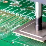
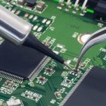
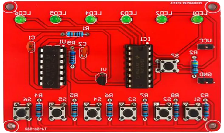
A reliable sensor PCB manufacturer plays an important role in developing electronic products that need accurate environmental sensing, data acquisition, signal processing, and real-time monitoring. A sensor PCB integrates one or more sensing devices with signal-conditioning circuits, processors, communication interfaces, power-management components, and other electronic devices on a compact printed circuit board.
Depending on the application, a sensor circuit board can detect temperature, pressure, humidity, light, acceleration, vibration, motion, or other physical conditions. The collected information is converted into electrical signals and processed by a microcontroller, processor, or other control system.
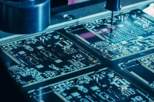
For projects requiring both bare-board fabrication and electronic assembly, customers can use PCB Manufacturing and PCB Assembly services to develop a complete sensor electronics solution.
What Is a Sensor PCB?
A sensor PCB is a printed circuit board designed to connect and control sensors while processing the signals generated by those sensing elements. It can include analog front-end circuits, amplifiers, filters, analog-to-digital converters, microcontrollers, communication interfaces, power supplies, and protection components.
Unlike a conventional PCB used primarily for general electronic interconnection, a sensor board must often maintain high signal integrity and stable electrical performance because even small amounts of noise, interference, temperature variation, or mechanical stress can affect measurement accuracy.
A well-designed sensor circuit board can combine multiple sensing functions into a compact electronic platform. Depending on the product architecture, it can operate as an independent sensing module or communicate with a larger control system through interfaces such as I²C, SPI, UART, CAN, RS-485, Ethernet, or wireless communication modules.
Types of Sensors Integrated Into PCBs
Temperature Sensors
Temperature sensing is one of the most common applications of sensor electronics. Thermistors, resistance temperature detectors, and thermocouples can be integrated with signal-conditioning circuits to provide temperature monitoring and control.
Thermistors are suitable for compact and cost-sensitive applications, while thermocouples are frequently used in industrial environments where a wide temperature range is required.
Pressure Sensors
Pressure sensors convert mechanical pressure into electrical signals. Piezoelectric and capacitive sensing technologies are commonly used in industrial equipment, automotive electronics, medical devices, and consumer products.
The PCB must provide appropriate signal conditioning and stable power to maintain reliable pressure measurements.
Motion Sensors
Motion-related applications commonly use accelerometers and gyroscopes. Accelerometers measure linear acceleration, while gyroscopes measure angular velocity and rotational movement.
These sensors are widely used in navigation systems, robotics, drones, industrial equipment, automotive electronics, and portable electronic products.
Optical Sensors
Photodiodes and phototransistors convert light into electrical signals. They can be used for ambient-light detection, optical measurement, automatic lighting, security equipment, and industrial monitoring.
Because low-level optical signals can be sensitive to electromagnetic interference, careful PCB layout and grounding are important during sensor PCB manufacturing.
Humidity Sensors
Humidity sensors are commonly based on capacitive or resistive sensing principles. They are used in environmental monitoring, HVAC equipment, smart appliances, industrial control systems, and other applications where humidity must be continuously monitored.
Key Sensor PCB Design Considerations
Designing a reliable sensor PCB requires more than simply placing sensors and electronic components on a board. Electrical, mechanical, thermal, environmental, and manufacturing factors must be considered together.
Signal Integrity and Noise Control
Sensor signals can be relatively small and sensitive to interference. PCB designers should therefore carefully manage trace routing, grounding, power distribution, return paths, and filtering.
Sensitive analog circuits should be separated from high-speed digital circuits and high-current switching paths where appropriate. Short and direct signal paths can also help reduce unwanted noise and signal degradation.
For complex designs, PCB Capabilities such as controlled impedance, fine-pitch fabrication, multilayer construction, and advanced PCB materials can help support demanding signal requirements.
Material Selection
The PCB material directly affects electrical performance, thermal stability, mechanical strength, and long-term reliability.
FR-4 is widely used for general-purpose sensor electronics because it provides a practical balance between electrical insulation, mechanical performance, thermal resistance, and cost.
For high-frequency or high-speed sensor systems, specialized materials such as Rogers or other high-performance laminates may be appropriate. Material selection should be based on operating frequency, dielectric requirements, temperature range, mechanical conditions, and overall product specifications.
Thermal Management
Temperature variation can affect both the PCB and the sensing element. Designers should consider component heat generation, thermal paths, copper distribution, heat dissipation, and the physical location of temperature-sensitive components.
For applications operating in high-temperature environments, selecting an appropriate laminate and component package can improve long-term stability.
Environmental Protection
Outdoor, industrial, automotive, and other demanding applications may expose a sensor circuit board to moisture, dust, vibration, chemicals, temperature cycling, or mechanical shock.
Depending on the application, protective measures may include conformal coating, appropriate enclosure design, sealed connectors, corrosion-resistant finishes, and robust mechanical mounting.
Miniaturization
Many modern sensors must fit into increasingly compact products. Miniaturization can require smaller components, finer traces, multilayer boards, HDI structures, microvias, and carefully optimized component placement.
A professional engineering review before production can identify manufacturing risks and help balance board size, reliability, performance, and cost.
Sensor PCB Manufacturing Process
A professional sensor PCB manufacturer should maintain controlled processes from engineering review through final inspection. A typical production workflow includes the following stages.
1. Schematic and PCB Layout
The design begins with the electrical schematic and PCB layout. Designers define sensor connections, power requirements, signal paths, communication interfaces, mounting holes, and component locations.
Design-for-manufacturing and design-for-assembly reviews can identify potential issues before fabrication.
2. Material Selection and Stack-Up
The appropriate laminate, copper thickness, dielectric thickness, and layer structure are selected according to the electrical and mechanical requirements of the application.
For multilayer sensor boards, stack-up design is particularly important for power distribution, grounding, signal integrity, and impedance control.
3. Imaging and Etching
During PCB fabrication, circuit patterns are transferred onto copper layers using imaging processes. Unwanted copper is removed during etching, leaving the required conductive traces.
4. Lamination
For multilayer boards, individual inner layers and insulating materials are aligned and laminated under controlled temperature and pressure.
Proper lamination is essential for maintaining dimensional stability and reliable interlayer connections.
5. Drilling and Copper Plating
Mechanical or laser drilling creates holes for through-hole components and vias. Copper plating is then used to establish electrical connections between appropriate PCB layers.
Advanced fabrication capabilities can support fine-pitch structures and small vias required by compact sensor designs.
6. Surface Finishing
Surface finishes such as ENIG, HASL, OSP, immersion tin, or immersion silver may be selected according to component requirements, soldering processes, environmental conditions, and product life-cycle expectations.
7. PCB Assembly
After bare-board fabrication, components can be installed using SMT, through-hole technology, or a combination of both.
For designs that combine different component technologies, Mixed Technology PCB Assembly can provide a suitable manufacturing solution.
Automated placement and controlled soldering processes help achieve consistent component positioning and solder-joint quality.
8. Inspection and Testing
Quality control is critical for sensor electronics because manufacturing defects can directly affect measurement performance.
Depending on the product, inspection may include AOI, SPI, X-ray inspection, visual inspection, electrical testing, and functional testing.
For development-stage products, Prototype PCB Assembly can help engineers validate component selection, PCB layout, assembly processes, and product functionality before moving into larger-scale production.
Applications of Sensor PCBs
The demand for sensor PCB manufacturing continues to grow as more products incorporate sensing, monitoring, automation, and connected intelligence.
Consumer Electronics
Smartphones, wearable devices, smart appliances, and portable electronics use sensors for motion detection, environmental monitoring, light detection, and other functions.
Compact sensor boards allow manufacturers to integrate multiple sensing functions into increasingly small product designs.
Industrial Automation
Industrial systems use sensor boards for temperature monitoring, pressure measurement, vibration detection, equipment monitoring, process control, and safety systems.
Reliable sensing can help manufacturers monitor machine conditions, improve production efficiency, and detect abnormal operating conditions.
Automotive Electronics
Automotive applications use sensors for vehicle control, safety systems, environmental monitoring, position detection, pressure monitoring, and driver-assistance functions.
Automotive sensor electronics must often withstand vibration, temperature changes, electrical noise, and other demanding operating conditions.
Medical Electronics
Medical and healthcare equipment can use sensor boards for physiological monitoring, temperature measurement, pressure measurement, patient monitoring, and diagnostic systems.
These applications generally require careful component selection, manufacturing control, traceability, and testing.
Smart Home and IoT Devices
Connected devices increasingly rely on sensors to collect real-time information about temperature, humidity, motion, light, and other environmental conditions.
A compact sensor circuit board can integrate sensing, processing, communication, and power-management functions into a single module.
Challenges in Sensor PCB Development
Miniaturization and Component Density
Reducing PCB size while maintaining reliable electrical performance can increase routing complexity and manufacturing difficulty. Fine-pitch components and high-density interconnect structures may be required for compact products.
Signal Interference
Multiple sensors and communication circuits operating on the same board can introduce electromagnetic interference and signal coupling. Proper grounding, shielding, filtering, layer planning, and trace routing are therefore essential.
Thermal and Environmental Stress
Sensor electronics can experience temperature cycling, vibration, humidity, dust, chemicals, and mechanical stress depending on the application.
Material selection, protective coatings, mechanical design, and appropriate testing can improve product durability.
Manufacturing Consistency
A sensor may require tighter electrical and mechanical tolerances than a conventional control board. Consistent fabrication, component placement, soldering, inspection, and testing are therefore essential for maintaining repeatable performance.
Why Choose GOPCBA for Sensor PCB Manufacturing?
When selecting a sensor PCB manufacturer, customers should evaluate not only PCB fabrication capability but also engineering support, assembly capability, testing, quality management, and production scalability.
GOPCBA provides integrated PCB fabrication and assembly services for projects ranging from prototypes to production. Its manufacturing capabilities include multilayer PCB fabrication, high-frequency PCB technology, controlled impedance solutions, flexible and rigid-flex PCBs, and other specialized PCB technologies.
For complete electronic manufacturing requirements, PCBA Capabilities include SMT, through-hole, mixed assembly, BGA assembly, turnkey manufacturing, inspection, conformal coating, and other assembly services.
GOPCBA also supports engineering activities such as DFM review, DFA analysis, BOM verification, Gerber review, component availability analysis, and prototype manufacturing support.
For projects that require material sourcing, PCB fabrication, component placement, testing, and delivery through one manufacturing partner, Turnkey PCB Assembly can simplify supplier management and production coordination.
Quality and Manufacturing Support
A dependable sensor PCB manufacturer should maintain quality controls throughout engineering, fabrication, assembly, and testing rather than relying only on final inspection.
GOPCBA states that its quality management approach covers PCB design, DFM checking, new product introduction, PCBA manufacturing, supply-chain management, testing, and personnel training.
Its manufacturing capabilities also include 100% electrical testing and a range of PCB technologies and materials for demanding applications.
For customers who need a complete production partner, the Why Choose Us page provides additional information about GOPCBA’s PCB manufacturing, assembly, component sourcing, equipment, delivery, and quality capabilities.
How to Choose the Right Sensor PCB Manufacturer
Before selecting a supplier, consider the following factors:
PCB Fabrication Capability
Confirm that the manufacturer can support the required layer count, trace width and spacing, copper thickness, material type, via technology, surface finish, and board dimensions.
Sensor PCB Assembly Capability
Check whether the supplier can assemble the required sensor packages, fine-pitch components, BGA/QFN devices, connectors, and mixed SMT/THT components.
Testing Capability
Ask about AOI, SPI, X-ray, electrical testing, functional testing, and other inspection methods relevant to the application.
Engineering Support
A capable engineering team should be able to review Gerber files, BOMs, stack-ups, component placement, manufacturing tolerances, and potential DFM risks before production.
Production Scalability
The supplier should be able to support the complete product life cycle, from prototype quantities to low-volume production and larger manufacturing programs.
Get Started With Your Sensor PCB Project
Whether you are developing a compact IoT device, industrial monitoring system, automotive electronics, medical equipment, or another sensing application, selecting the right sensor PCB manufacturer can significantly influence product reliability, development time, and manufacturing cost.
GOPCBA provides PCB fabrication, PCB assembly, engineering support, component sourcing, testing, and related electronics manufacturing services. Customers can Contact GOPCBA to discuss their PCB requirements and submit project information for evaluation.
Frequently Asked Questions About Sensor PCBs
What is a sensor PCB?
A sensor PCB is a printed circuit board that integrates sensors with electronic circuits for signal acquisition, processing, communication, and power management.
What materials are commonly used for sensor PCBs?
FR-4 is widely used for general applications. High-Tg, high-frequency, aluminum-backed, flexible, and other specialized materials may be selected according to electrical, thermal, mechanical, and environmental requirements.
What types of sensors can be installed on a PCB?
Common examples include temperature sensors, pressure sensors, humidity sensors, accelerometers, gyroscopes, photodiodes, phototransistors, and other application-specific sensing devices.
What is the difference between a sensor PCB and a sensor module?
A sensor PCB refers primarily to the printed circuit board and its integrated electronics, while a sensor module may include the PCB, sensors, enclosure, connectors, firmware, and other mechanical or electronic components as a complete functional unit.
How is a sensor PCB tested?
Testing can include visual inspection, AOI, SPI, X-ray inspection, electrical testing, continuity testing, and functional testing. The exact test strategy depends on the design and application.
How can I reduce interference on a sensor PCB?
Use appropriate grounding, power filtering, signal separation, shielding, controlled routing, short sensitive traces, suitable stack-up design, and careful separation between analog, digital, and high-current circuits.
Can sensor PCBs be produced in small quantities?
Yes. Prototype and low-volume production can be used to validate the design before scaling to larger production quantities. This approach can reduce development risk and identify manufacturing issues early.
What information is required for a sensor PCB quotation?
Typical manufacturing information includes Gerber files, PCB specifications, BOM, pick-and-place files when assembly is required, drawings, special material requirements, quantities, testing requirements, and other technical documentation.