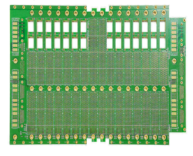
Annular Ring Requirements and Design Rules
The annular ring is the copper that remains around a drilled hole after the drill has taken its share of the pad. It carries the connection between the hole and the trace, and if it is too small the result is a breakout, a weak barrel, or an intermittent joint. Sizing it correctly means allowing for every source of misregistration and then adding a margin, which is why the smallest ring that a fabricator can hold is not the same as the ring a design should specify.
What the Ring Has to Do
Mechanically, the ring holds the barrel to the pad and distributes the stress that appears when the board expands during reflow. Electrically, it provides the connection to the trace and contributes to the current carrying capacity of the joint. Where the ring is thin on one side, the barrel can separate from the pad under thermal cycling, and the failure appears as an intermittent open rather than a clean break.
The ring also has to survive the drilling process and the plating process. A hole that is drilled off centre removes more copper from one side, and a pad that is smaller than the drill’s positional tolerance will break out. Because the drill position and the pad position both vary, the ring is a statistical result rather than a fixed dimension.
The Sources of Misregistration
Several tolerances add up. The drill machine has a positional accuracy, often around 50 to 75 microns for a modern machine. The imaging and etching of the pad have their own tolerance, and the layer to layer registration of a multilayer board adds another. The laminate itself moves during lamination and during the drilling that follows, and the amount depends on the material and the panel size.
Because the contributions are independent, the total is calculated as a root sum square rather than as a simple sum. A board with a drill tolerance of 75 microns, an imaging tolerance of 50 microns, and a layer registration of 50 microns has a combined tolerance of about 100 microns, which must be divided between the two sides of the hole. The ring on each side must be at least that figure plus the required minimum.

Minimum Ring for Inner and Outer Layers
Inner layers usually require less copper than outer layers because the barrel is supported by the laminate on both sides. Common requirements are 50 microns minimum for a class 2 board and 25 microns for a class 3 board on inner layers, measured at the thinnest point. Outer layers are often specified at a larger figure because the pad must also survive the surface finish and the soldering process.
The class of the board is the reference. A general purpose product can accept a smaller ring with a higher statistical breakout risk, while a high reliability product requires a larger ring and a tighter process. Where the finished board must meet a specific standard, the requirement should be quoted from that standard rather than chosen by preference, because an audit will measure the actual ring rather than the drawing.
Choosing a Pad Size
The pad diameter is the drill diameter plus twice the ring. Where the drill tolerance is 100 microns combined, a minimum ring of 50 microns and a drill of 0.3 mm give a pad of 0.5 mm, which is a simple calculation. The difficulty is that the same pad must also satisfy the soldering process, and a pad that is small for soldering reasons may be at the limit for the ring.
In practice, the ring is often the constraint that decides the pad. Reducing drill sizes is the usual way to gain space, and a smaller drill reduces both the hole and the pad. Where a design must place a dense array of vias, a smaller drill with a controlled ring gives more routing space than a larger drill with a generous ring, which is one of the reasons fine pitch designs use small vias.

Breakout and Its Consequences
A breakout occurs when the drill cuts beyond the pad so that the ring is only partly present. A small breakout on an inner layer may be acceptable if the copper remaining still meets the minimum ring, but a breakout on an outer layer that exposes the barrel usually fails inspection. The ring also contributes to the current carrying capacity of the joint, so a hole that carries significant current should be sized on that basis as well as on the mechanical tolerance. The failure is not only cosmetic, because the exposed barrel edge is a place where plating adhesion is weakest.
Where a breakout is unavoidable, the design should be changed rather than the acceptance criterion relaxed. Moving the via, enlarging the pad, or reducing the drill diameter are all preferable to accepting a marginal ring, because the defect will appear at a rate determined by the process distribution and will be invisible on most of the boards produced.
Testing and Verification
The ring is verified by microsection at first article and periodically thereafter. The section is measured at several points around the hole, because the thinnest point is what matters and it is rarely where it is expected. Where a panel contains many hole sizes, the largest and the smallest are the ones that reveal the process capability most clearly.
In-process verification also matters. A drill that has wandered because of a worn bit or an incorrect program will show as a shift in the ring position across a panel. Measuring a few holes from different areas shows whether the error is systematic or random, which directs the corrective action to the machine, the program, or the bit.
Where a design is dense, the temptation is to specify the smallest ring that the fabricator says it can hold. A better approach is to ask for the process distribution and to set the design limit so that a defined fraction of holes remains inside it. That converts a capability claim into a design decision with a known yield consequence.
Design Rules That Avoid Trouble
Keep every hole at least one pad radius away from the edge of a plane or another pad, so that the drill’s positional tolerance has room. Avoid placing a via on a narrow trace where the pad has to grow beyond the trace width, and where a via must be small, use a filled and capped construction rather than pushing the ring to its limit. Provide a keep-out region around a hole in a ground plane rather than relying on the plane to supply the ring.
Document the requirement. A note on the fabrication drawing that states the minimum ring for inner and outer layers, and the standard that applies, gives the fabricator a measurable target. Combined with a sensible pad size and a controlled drill process, it produces boards that pass microsection on the first attempt. The pad design standards and manufacturability rules cover the same calculation from the layout side.
Related reading: our fabrication notes, board quality and design release notes cover the same ground.
FAQ
What is the minimum annular ring? Around 50 microns at the thinnest point for a class 2 board and 25 microns for class 3 on inner layers is typical, with more on outer layers. The applicable standard should be quoted rather than assumed.
Does a smaller drill always give more routing space? Usually, because the pad shrinks with the hole. The limit is the plating aspect ratio, since a very small hole in a thick board is difficult to plate uniformly.
Is a small breakout acceptable? Only if the remaining copper still meets the minimum ring and the applicable standard allows it. Enlarging the pad or reducing the drill is the safer response.