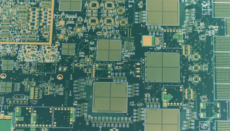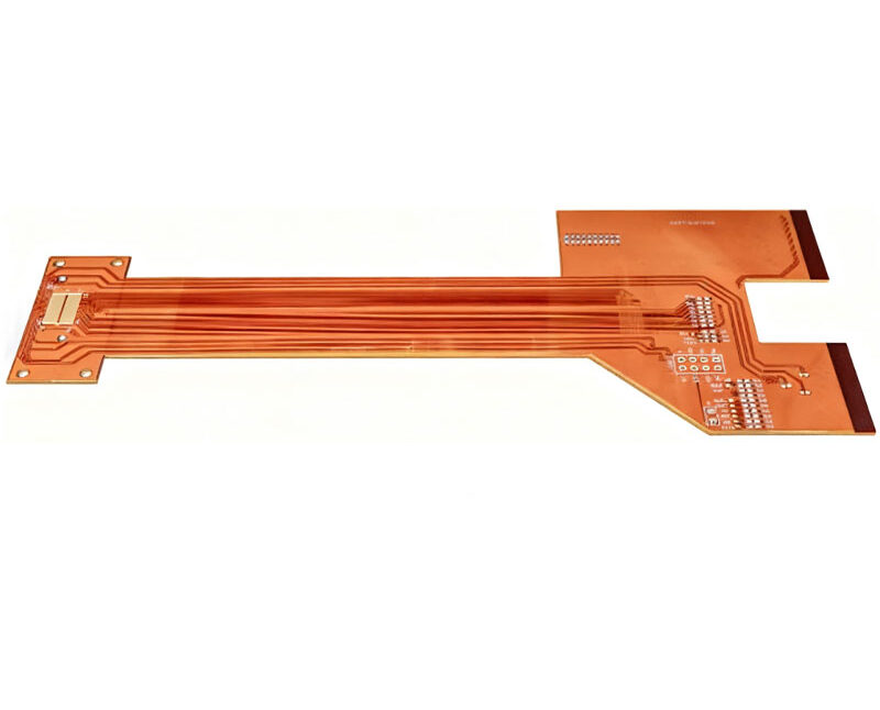
Interconnect Stress Testing of PCB Vias and Plated Holes An interconnect stress test passes a current through a chain of vias to heat them, then cools them, and repeats the cycle while measuring the resistance of the chain. The resistance rises as a barrel begins to crack, and the test…

Process Water Treatment in PCB Manufacturing Water is the largest material a board shop consumes and the one it thinks about least, until a plating defect or an effluent limit forces the subject. Process water touches the panels at almost every step, and its quality determines whether a rinse removes…
Inner Layer Oxide Treatment Before Lamination Before the layers of a multilayer board are pressed together, the copper on the inner layers is treated so that the resin can bond to it. Copper alone does not bond well to epoxy: the surface is smooth and chemically unreactive, and a bond…
Thermal Interface Material Dispensing Control on Assemblies A thermal interface material fills the microscopic gaps between a component and its heat sink, and its purpose is to replace the air that would otherwise occupy those gaps. Air is a poor conductor, so the interface is often the largest single resistance…
Board Level Shield Can Design And Attachment A board level shield is a metal cover placed over a group of components to stop the radio frequency energy they generate from leaving the area and to stop external energy from reaching them. It is a mechanical part fitted to the board,…
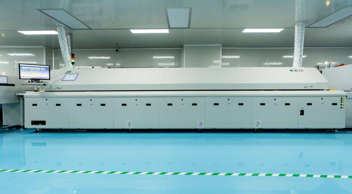
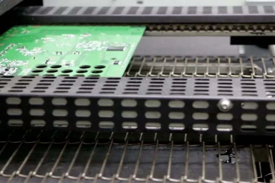
Vacuum Reflow Soldering for Solder Void Reduction on BGA A void is a bubble of gas trapped inside a solder joint, and in most joints it is harmless. In a joint that has to conduct heat, however, a void reduces the area through which the heat can pass, and a…
Outsourcing Decisions in PCB Manufacturing An outsourcing decision is a make or buy question, and in a board shop it is usually triggered by capacity rather than by strategy. The enquiry that arrives when the drilling area is already full, the technology that sits just beyond the shop’s capability, or…
Edge Castellation Design For Module Boards A castellation is a plated half hole at the edge of a small board, formed by drilling a full hole at the board outline so that the saw or the router cuts through it and leaves a semicircular plated recess. The connections from the…
Hatch Plane Design On PCB Layers A hatch plane is a copper area filled with a grid of lines rather than with solid copper. It carries the same net as a solid plane and it is connected the same way, but the material is removed in a regular pattern, which…
Glass Fabric Selection and Its Effect on PCB Laminates A laminate is a sandwich of glass fabric and cured resin, and the fabric is the part that most designers never consider. The weave style, the yarn count and the amount of resin around the glass determine the thickness, the mechanical…