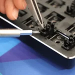
Edge Castellation Design For Module Boards
A castellation is a plated half hole at the edge of a small board, formed by drilling a full hole at the board outline so that the saw or the router cuts through it and leaves a semicircular plated recess. The connections from the module to the carrier board are then made by soldering into those recesses, which allows a module to be mounted flat with no connector and no through hole pins.
This article covers how a castellation is formed, how it is dimensioned for a reliable joint, and how the plating and the cut are controlled.
How A Castellation Is Formed
The hole is drilled and plated as a normal plated through hole, in a position that places its centre on the board outline so that half of the hole lies inside the board and half outside. When the outline is cut, whether by routing or by scoring, the cut passes through the plating and leaves a plated semicircular wall exposed at the edge. The exposed plating is what the solder wets, and the copper of the internal layer connects to it as it would to any other plated hole.
Because the hole is cut after plating, the plating has to be thick enough to survive the cutting without tearing, and the cut has to be made without smearing the plating into the neighbouring surface. The quality of the resulting edge is one of the things a castellated module is judged on, and it is a consequence of the drilling, the plating and the cut rather than of any separate operation. Plating defects that would be invisible inside a board become visible here, and their prevention is described under copper plating defects prevention.
Dimensioning For A Joint
The dimension that matters is the width of the exposed plating at the edge, which is the diameter of the original hole, and the height over which it is exposed, which is the board thickness. Together they set the area available for the solder fillet. A castellation that is too small does not accept enough solder for a reliable joint, and one that is too large takes space that the module does not have.
The pad around the castellation on the module is normally the annular ring that remains, and it should be wide enough to give the fillet somewhere to spread. Where space is tight, the ring is kept small and the joint relies on the recess alone, which makes the process more sensitive to the amount of paste and the profile. The pad conventions that apply are the same as for any other joint, and they are described under PCB pad design standards.

The Cutting Operation
The cut through the castellation is made with a router or a scoring wheel, and both have an effect on the result. A router leaves a milled surface and a small burr where the plating is cut; the burr has to be removed without removing the plating, which is a balance that is set by the bit condition and the cut parameters. Scoring leaves a cleaner edge and a smaller burr but cannot follow a curved outline, so it is used only on a straight edge.
The cut depth relative to the hole is the variable that decides whether each castellation is half a hole or something else. A cut that is offset towards the inside of the board leaves more than half the hole and a wider contact area, and one that is offset outwards leaves less. The outline in the artwork is the nominal position, and its tolerance relative to the hole pattern is what the castellation tolerance depends on, so the two are specified together rather than separately.
Soldering The Module
The module is placed on the carrier board with its castellations over matching pads, and the joints are made by reflow or by hand. The key process requirement is that the solder reaches the recess and forms a fillet on both the recess and the pad, which means the paste volume and the profile have to be adequate for a joint that is partly vertical. A castellation joint that has wetted only on the pad and not on the recess looks acceptable from above and has a fraction of the intended strength.
Inspection from the side is the check that confirms the fillet, and it is the reason the joint should be accessible. Where the module is surrounded by tall components or by a shield, that access is lost and the inspection becomes an X-ray question. Designing the carrier board so that the module edge is exposed after assembly is therefore a functional requirement rather than a convenience. The mechanical arrangement around the module is part of the general layout described under board outline and mounting design.
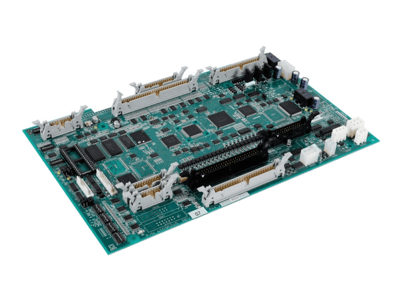
Design Considerations For Modules
A module that uses castellations has to accept that its edge is its connector. That means the edge cannot be used for anything else, the outline dimension has a direct effect on the joint, and the module has to be handled by its faces rather than its edges after assembly. The pitch of the castellations is limited by the hole size that can be plated and cut reliably, and it is coarser than the pitch of a fine pitch connector.
Castellations also impose a routing constraint on the carrier. The pads have to be laid out to match the module exactly, and the tolerance stack between the module outline, the castellation position and the carrier pads is what decides whether the solder wets both surfaces. A generous pad that extends beyond the castellation in both directions absorbs part of that stack and is usually worth the space.
Verification
Verification of a castellated module is partly dimensional and partly visual. The edge is inspected for complete plating around each recess, for burrs and for plating that has peeled at the cut. The dimensional check confirms the position of each castellation against the outline, which is the figure that determines whether the carrier fits. A section through a castellation shows the plating thickness and whether the barrel is intact after cutting.
On the assembled product the check is the fillet, seen from the side, and the mechanical strength as measured by a shear test on a sample. The shear test is the more informative of the two, because a joint that has wetted both surfaces but with insufficient volume fails at a lower load than one with a full fillet, and the difference is not always visible.
Additional Considerations for This Build
Practical attention to edge plating pays for itself here, because it decides whether the finished board behaves as the drawing intended. Where the requirement is not stated on the fabrication drawing or in the assembly notes, the shop has to assume a default, and that default is rarely the value the design was simulated with. Stating edge plating explicitly, together with the tolerance that applies, removes the assumption and keeps the result predictable from batch to batch.
FAQ
Why use castellations instead of a connector? They remove the connector from the module, which saves height and cost and allows the module to be soldered in the same reflow as the rest of the assembly. The trade is a coarser pitch and a joint that is harder to inspect.
Can a castellation be repaired? It can, with a fine tip and a local flux, but the joint is partly vertical and difficult to reheat. The repair is usually done from the side and verified visually, which makes access a design requirement.
How is the castellation position toleranced? Relative to the board outline, with the outline and the hole pattern specified together. The tolerance of each alone is not enough to predict whether the joint will form on the carrier.