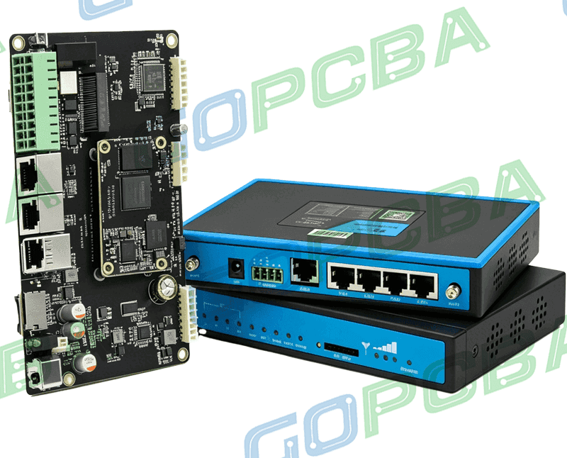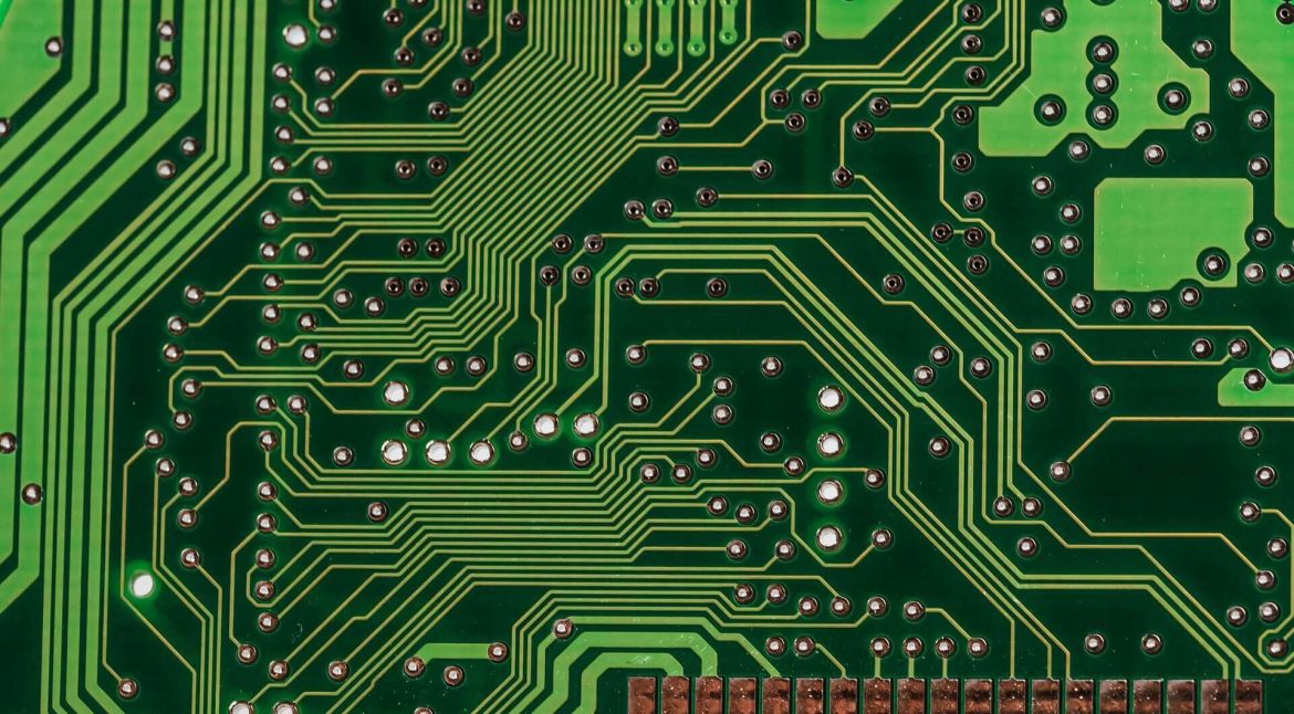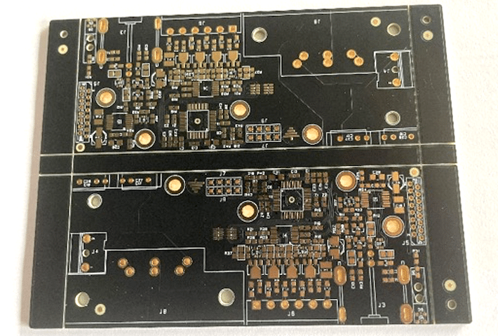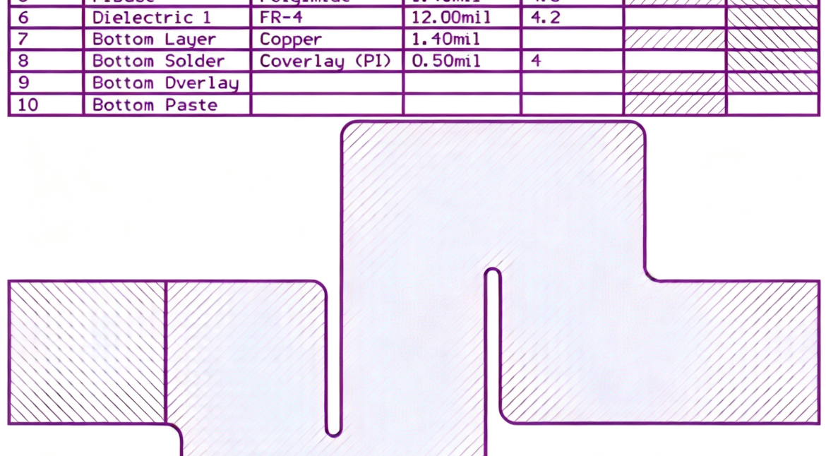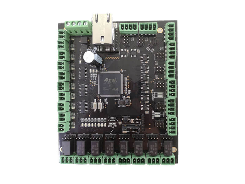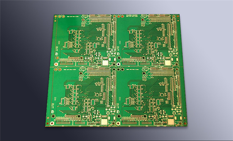
Castellated Holes and Module Edge Design for PCB Modules A module that solders onto a carrier board like a component has no pins and no connector. Its interface is a row of castellated holes along the edge, each one a plated half cylinder that wets to a pad on the…
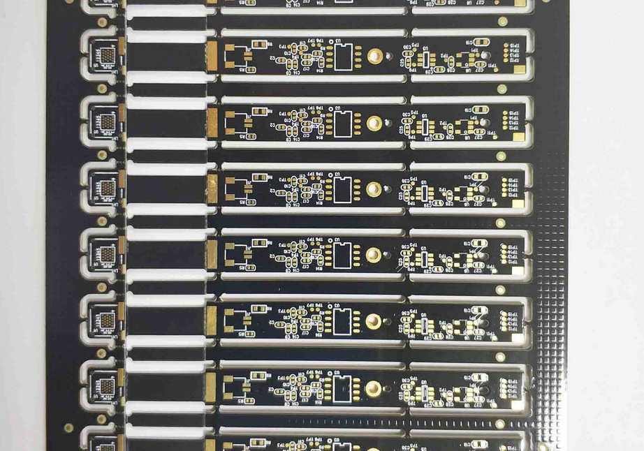
Heavy Copper PCB Design and Etching Tolerance Explained Heavy copper boards look simple to design because the traces are wide and the geometry is coarse. In practice they behave like a different process. The etch that shapes a one ounce layer cannot shape a four ounce layer in the same…
Safety Critical PCB: Safety Critical System PCB: Standards, Materials and Testing A safety critical system is one where a failure can cause injury, and the boards inside such systems are designed so that a failure either does not occur or occurs in a way that is detectable and safe. That…
AI PCB Assembly in Robotics, IoT and Smart Devices Assembly has always been a data-rich process, and for most of its history that data was used after the fact, in yield reports and failure analyses. That is changing. AI PCB assembly shifts the same information into the process itself, using…
Practical Notes on ESP32-C3 Vs ESP32-S3 Two of the most popular Espressif parts look similar on a pinout diagram and behave very differently once they reach the layout stage. The ESP32-C3 vs ESP32-S3 question comes up constantly in design reviews, and the usual answer about core count and price misses…
Practical Notes on Embedded Copper Coin Power density keeps rising in electric vehicle controllers, AI accelerator cards, industrial inverters and telecom power amplifiers, and the weakest link in those designs is often the path heat takes out of the die. An embedded copper coin PCB attacks that problem at the…
Practical Notes on Rogers 6002 When a design moves into millimeter wave territory, the laminate stops being a background detail and becomes part of the circuit. Rogers 6002 is a ceramic filled PTFE composite built for that situation, with a dielectric constant near 2.94 and a dissipation factor low enough…
Practical Notes on Plasma Etching Vs Chemical Etching Every copper pattern on a printed circuit board is defined by removing material, and the way that removal happens decides how fine the traces can be, how clean the surface ends up and how much the board costs. The comparison of plasma…
Laser Soldering vs Reflow Soldering: Choosing the Right Process Both processes melt solder to form a joint, and beyond that they have almost nothing in common. Reflow soldering brings an entire assembly up to temperature in a controlled oven, while laser soldering delivers energy to one joint at a time…
HDI Failure Beyond Microvia Cracks: Resin Starvation and CAF When engineers discuss reliability in high density interconnect boards, the conversation usually goes straight to microvia cracks. Thermal cycling, expansion mismatch and copper fatigue are real mechanisms, well documented and increasingly well managed through better materials and tighter design rules. They…