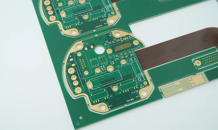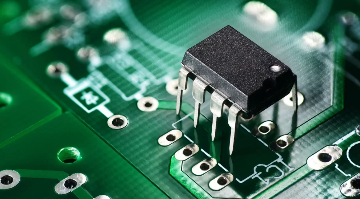
Charger PCB Price Guide: Board, Copper and Finish Costs A charger board is one of the few PCBs where cost, safety and thermal performance are judged together. Buyers who ask only for a unit price usually come back with a re-quote, because the real number depends on stackup, copper weight,…
PCB Thermal Design: Placement, Reliefs and Symmetry Heat is generated in a few small places on a board and has to leave through the whole of it. Thermal design is the business of arranging those places so that the heat finds a path out, and arranging the parts that cannot…
Rogers Selective Hybrid Lamination for High Frequency Boards High frequency laminate is expensive, and a board seldom needs it everywhere. A product might carry a radio section, a long antenna feed and a fast serial link alongside a microcontroller, power conversion and a connector field that would work perfectly well…
Selective Surface Finish: ENIG and OSP on the Same Board Surface finish is usually specified as a single choice for the whole board, but some products genuinely need two. A design may require a flat, gold plated surface on a fine pitch connector and a cheap organic finish everywhere else,…
Hand-Made PCB Prototyping: Toner Transfer, Etching and Drilling Anyone can put a circuit together on a piece of laminate with a laser printer, an iron and a tray of etchant, and the exercise is worth doing at least once, because it makes the fabrication process visible. The steps below follow…
PCB Production Process Flow: Single-Sided, Double-Sided and Multilayer A production process flow for a printed circuit board is a sequence of operations in which every step prepares the surface, the geometry or the copper for the step that follows. The sequence differs by board type, but the rules underneath it…
PCB Routing Rules That Keep a Layout Clean Routing rules exist because the same mistakes appear on every board, and most of them can be prevented by a short list that the layout is checked against. A rule that is written down can be enforced by a design rule check,…
Via Stubs and Via Effects in High Speed Design A via looks electrically innocent on a schematic, and at low frequency it is. At multi gigabit rates it becomes one of the most significant discontinuities on the board, because the plated barrel is a capacitor, the unused portion below the…
Microwave PCB Fabrication: Materials, Tolerances and Tests A microwave PCB looks like any other printed circuit until the requirements are read. The tolerances are tighter, the materials are different, the vias behave as circuit elements rather than as connections, and the verification is performed with instruments that measure reflection rather…
Blood Pressure Monitor PCB Design: Signal Chain and Layout A blood pressure monitor is a good example of a product where the board is the instrument. The measurement depends on resolving a small pressure oscillation that sits on top of a much larger static pressure, and the difference between the…