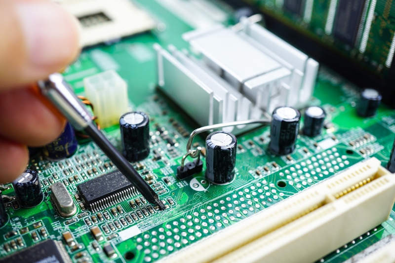
PCB Filter Circuit Design: Layout, Types and EMI Filtering A filter circuit is the part of a design that decides which frequencies are allowed to travel and which are turned away. On a board it appears in many forms, from a capacitor beside a power pin to a multi element…

PCB Differential Signaling: Impedance and Length Matching Differential signaling sends one signal down two traces instead of one and recovers the data from the voltage between them rather than from the voltage to ground. That one change buys immunity to a large class of interference, but it also imposes rules…
PCBA Capability: How to Judge a Manufacturer Process Two assembly houses can quote the same board within a few percent of each other and deliver very different products, because the quotation says nothing about the capability behind it. PCBA capability is measurable, though: it shows up in the smallest package…
PCB Plating Cost: Copper, Nickel and Gold Per Area Plating is one of the few PCB processes where the raw material price is set by a global commodity market, and that makes it unusually sensitive to thickness, area and the metal involved. A board that needs a gold edge connector…
FPGA Design Flow from Entry to Configuration An FPGA design is built in stages that run in a fixed order, and each stage exists because the one before it cannot answer the question the next one asks. Code can be simulated but not placed; a netlist can be placed but…
Via-in-Pad Solder Wicking: Causes and Prevention Putting a via directly inside a component pad is one of the most effective ways to escape a dense BGA or a fine pitch package, and it is now routine in high density interconnect work. It also creates a path for molten solder to…
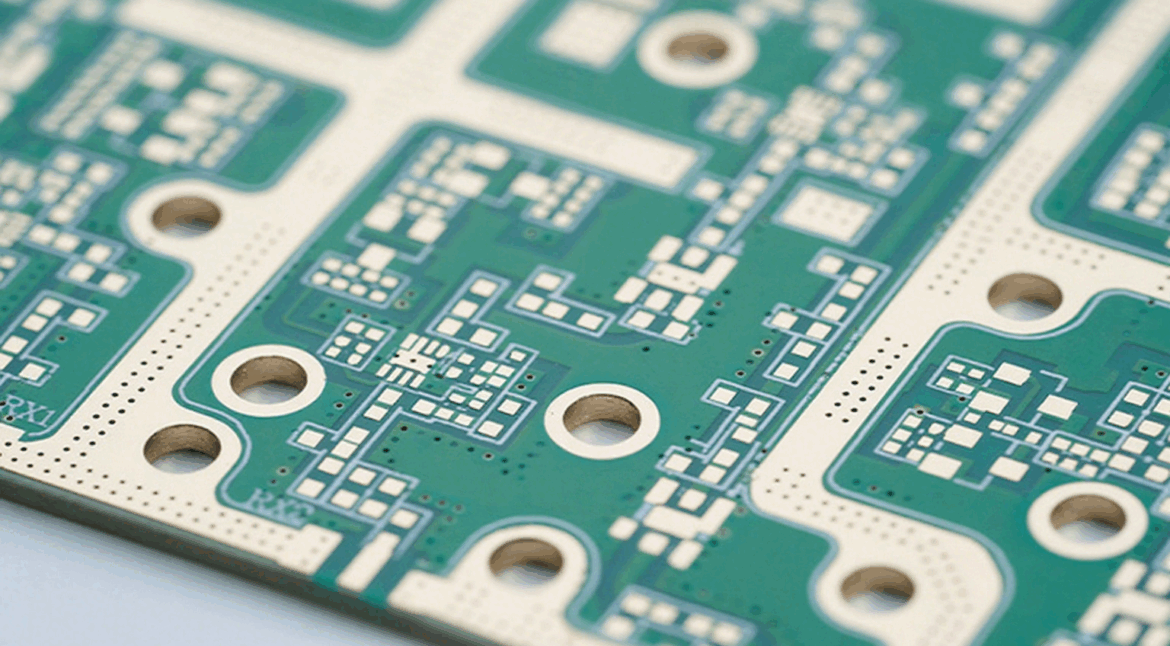
PCB Manufacturing Parameters and Standards Explained A fabrication drawing is only useful if every number on it means the same thing to the designer and to the shop that builds the board. That is what a parameter list is for. Registration, hole tolerance, copper thickness, impedance and finish thickness all…
How Many Layers Does a High-Speed PCB Need? Layer count is the first number a high-speed PCB team has to commit to, and it is the one that is hardest to change later. Too few layers and the routing, the return paths and the power delivery all compete for the…
Acidic vs Alkaline Etching for PCB: Chemistry Compared Once the pattern has been imaged and developed, the panel still has to give up the copper that the resist does not protect, and that step is done in a wet chemistry bath. Two families dominate production: acidic etching, built around cupric…
BGA Rework: Equipment, Profiles and Yield A ball grid array hides its joints underneath the package, so it cannot be inspected or repaired in the way a leaded part can. When one of those joints fails, the board is not necessarily scrap: it can be taken back to the reflow…