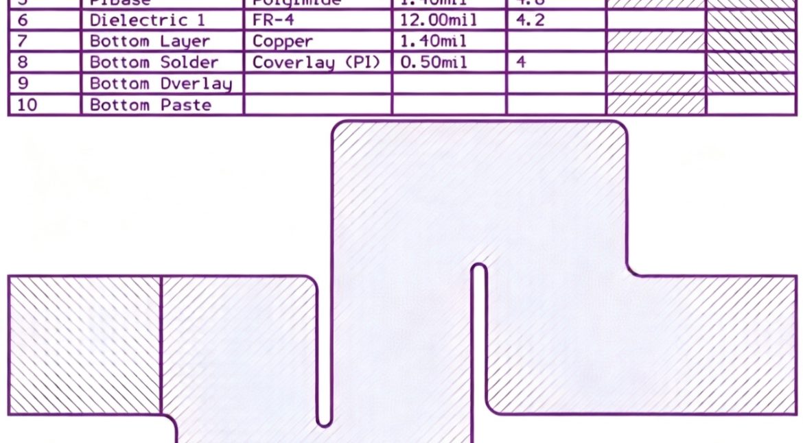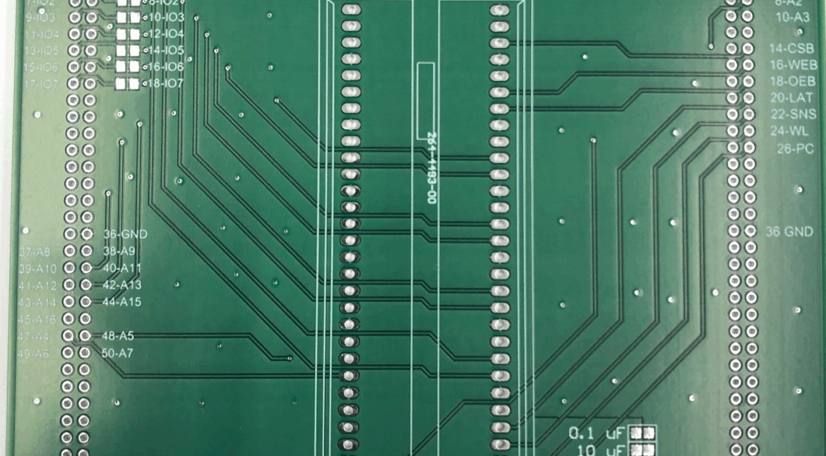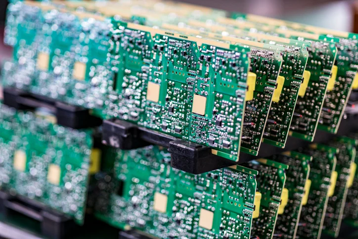
FR4 vs Mid-Loss Laminate: Dk, Df and Skew Compared Standard FR4 is the default laminate for the overwhelming majority of circuit boards, and its limits only become visible as data rates rise. Between the ordinary grade and the expensive low loss materials there is a middle family of modified epoxy…
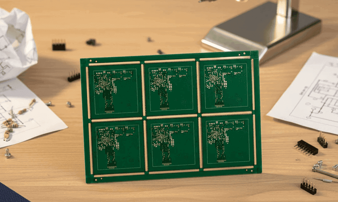
Via in Pad and Resin Plugging: Process and Design A via belongs between pads, not inside them. That is the normal rule, and it is the reason a ball grid array with a dense ball pitch can be impossible to escape: there simply is no room left between the pads…
ESD Protection at Board and Enclosure Level Static discharge is a fast, high-current event that lasts nanoseconds and arrives through paths the designer did not draw. It enters through a connector, a keypad, a seam in the enclosure or a metal part, and it leaves through whatever connection to earth…
10-Layer PCB Standard Thickness: What to Specify Ten layers is the point at which a board stops being an ordinary multilayer and starts needing a considered stackup. It offers enough layers for several signal groups, more than one power plane and the reference planes those signals need, and it is…
Grid Control PCB: Isolation, Surge and Reliability Design Equipment connected to an electricity network has to survive conditions that would destroy ordinary industrial electronics. Lightning induced surges, switching transients, voltage sags and faults that drive current far beyond the design value all arrive at the terminals, and the product is…
PCB Silkscreen: Design Rules and Ink Selection The silkscreen is the last process step on most boards and the one that receives the least design attention, which is why it is also a frequent source of manufacturing complaints. Ink printed over a pad ruins solderability, text that is too small…
High-Frequency PCB Materials and Hybrid Stackups A high-frequency PCB is usually described by its material rather than by its geometry, and that emphasis is correct. Once a signal spends a meaningful part of its energy in the laminate instead of the copper, the loss tangent of the dielectric, not the…
PCB Design Mistakes That Stop a Prototype at CAM When a prototype comes back late, the cause is usually not the fabricator. It is the data. A layout that passes every check inside the CAD tool can still stop at CAM, because the checks in the tool model the schematic…
COB LED vs SMD LED: Chip-on-Board Packaging and Thermal Design Two LED products can emit the same number of lumens and still behave nothing alike on a board. A COB LED bonds many dies directly to the substrate, while an SMD LED packages each die in its own housing and…
Switching Regulator PCB Layout: Loops, Grounding and Checks A switching regulator is a small circuit with a large appetite for current, and the layout decides whether that current stays where it was planned or sprays across the board. The electrical design can be textbook correct and the prototype still fail,…