Via in Pad and Resin Plugging: Process and Design
A via belongs between pads, not inside them. That is the normal rule, and it is the reason a ball grid array with a dense ball pitch can be impossible to escape: there simply is no room left between the pads for the vias that have to leave the array.
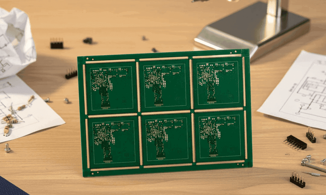
The way out is to drill the via inside the pad itself and then make the pad flat again. This article describes why that requires a resin plugging step, how the sequence runs, and the two process areas that decide whether the finished panel is flat: laminate selection and lamination control.
Why a Via Has to Be Drilled Inside a Pad
Escape routing from a fine-pitch array is a space problem. Each ball needs a via to reach an inner layer, and the vias need clearance from the pads and from each other. As the pitch falls, the space between pads falls faster than the pad size does, and at some point there is no legal position left outside the pad.
Placing the via in the pad resolves the geometry but creates a new problem. A drilled hole in a pad leaves a void, and a void under a solder joint behaves badly. Solder flows into the hole during reflow, drawing material away from the joint, which produces a void in the connection and, where the hole passes through to the other side, a solder protrusion that can short against whatever sits behind the board.
Where the via is not plugged, the failure mode is well known: insufficient solder on the ball, a weak joint, and in severe cases solder wicking through to the opposite side. The defect is intermittent, which makes it expensive to diagnose, and it appears on the joints that are most difficult to inspect.
<img src="https://www.gopcba.com/wp-content/uploads/2026/03/Automotive-PCB-Assembly.jpg" alt="Filled and plated via in pad on a BGA escape” />
Resin Plugging and the Sequence That Follows
The answer is to fill the hole with a resin that cures to a solid, and then to plate over it so that the filled via becomes indistinguishable from ordinary pad copper. The plugging is performed as a separate process step, and the standard sequence is: drill the vias that are to be plugged, plate them to make the barrel conductive, fill them with resin, cure the resin, and then grind the surface flat.
Two details decide whether the result is usable. The resin has to be filled without voids and without shrinking away from the barrel as it cures, which is why the curing profile is controlled rather than rushed. And the planarisation has to remove enough material to expose clean copper without cutting into the surrounding pad, which is a tolerance problem as much as a process one.
Plating Back to a Pad
Once the resin has been ground flat it is flush with the surface but it is not metal, so it cannot accept a solder joint. The plating and filling steps used in HDI construction are the same ones used here, and the same trade-offs apply. A further plating step deposits copper over the filled area, after which the pad is a continuous copper surface again and can be treated as an ordinary land.
The consequence for the designer is that the finished pad geometry has to be specified with the plugging in mind. The pad must be large enough to contain the via plus the annular ring and the plating allowance, and the solder mask opening must account for the fact that the surface has been planarised. A pad specified at the size that would be adequate for a via placed beside it will be marginal after plugging, especially on a tight pitch.
Laminate Types and How They Are Classified
Everything above happens on a laminate, and the laminate determines how well the mechanical steps go. A base material is a reinforcement, usually woven glass or paper, impregnated with a resin and dried to a partially cured state. In that state it is called a prepreg, and the layers of prepreg plus copper foil are pressed and cured into the finished core.
The families are named after the resin. Phenolic and epoxy systems dominate rigid boards, with epoxy the standard for anything that has to survive soldering. Polyimide and polytetrafluoroethylene are used for flexible circuits and for high-frequency work respectively. Classification also runs along the other axis, by reinforcement and by properties, which is why the same generic material can arrive with a wide range of glass transition temperatures, dielectric constants and loss tangents.
Prepreg Orientation and Lamination Control
A woven reinforcement does not shrink equally in both directions when it is pressed. The warp direction, which runs along the roll, behaves differently from the weft, which runs across it. If the prepreg sheets in a stack are laid up with their directions mixed, the panel will shrink unevenly and bow or twist as it cools.
The practical rule is to keep the orientation consistent through the stack and to record it in the lay-up drawing. This is one of the more common causes of board warpage, and it is invisible on the finished board, which makes it difficult to diagnose after the fact. The same lay-up document should state the number and type of prepreg sheets at each interface, because that is what controls the dielectric thickness and, through it, the impedance of any controlled net.
Warpage Causes and What Can Be Recovered
Warpage has several sources: uneven copper distribution between the two sides of the board, mismatched prepreg orientation, a lamination cycle with an aggressive heating or cooling rate, and the thermal shock of a hot-air solder levelling step followed by a fast quench. Thin panels are more sensitive than thick ones because their stiffness is lower in proportion to the stresses applied.
Some of it can be recovered. Boards that fail a flatness check are sometimes pressed flat in an oven under load and allowed to cool under that load, which relaxes the internal stress; a board that needs two or three cycles of this treatment is usually a sign that the process rather than the board is at fault. Where the underlying cause was a copper imbalance or a mixed prepreg orientation, however, the board will return to its bowed shape and the recovery is not permanent, as described in the notes on dimensional stability and expansion.
Design Rules for a Via-in-Pad Stack
The first rule is to use the process only where it is needed. A BGA whose pitch still permits vias between the pads should be escaped the conventional way, because every plugged via adds a process step and a plating operation. Restricting the technique to the rows where there is genuinely no alternative keeps the cost and the risk where they belong.
The second rule is to give the fabricator the information it needs to plan the sequence. The drill table should identify the plugged vias separately from the rest, and the drawing should state the tolerances that matter: the depth of the drilled hole, the flatness of the filled area, and the thickness of the plated copper over it. Any via that is filled and capped, or filled and plated over, should be specified as such rather than left to interpretation.
The third rule concerns the assembly side. A filled and plated via behaves like a solid pad, but only if the surface really is flat. The choice between a via in pad and a plated-through via is the first decision to make here. A via whose filler has shrunk slightly below the surface will trap flux and produce a void in the joint, and the defect will look like a paste problem rather than a board problem. Asking for a sample cross-section from the fabricator before the first production order is the cheapest way to confirm that the process is under control.
FAQ
Is a via in pad always plugged? For a soldered pad, yes. An unplugged via inside a pad will wick solder away from the joint and can produce a protrusion on the opposite side. Where the via is in a pad that is never soldered, such as a thermal pad under a device that is not reflowed, the requirement is different.
Does plugging raise the finished board thickness? No, provided the grinding step is performed correctly. The filler is levelled flush with the surrounding surface and then plated, so the finished thickness at that point matches the rest of the panel.
What causes a panel to bow after lamination? Uneven copper distribution, prepreg sheets laid up with mixed warp and weft directions, and an aggressive lamination or solder levelling cycle are the usual causes. The first two are design and lay-up decisions and cannot be corrected afterwards.