Thermal Via Arrays: Moving Heat Through the Board A thermal via array is the simplest thermal management tool available on a printed circuit board: a group of small vias under a component that carries heat from the pad into the copper layers below. It costs almost nothing in material and…
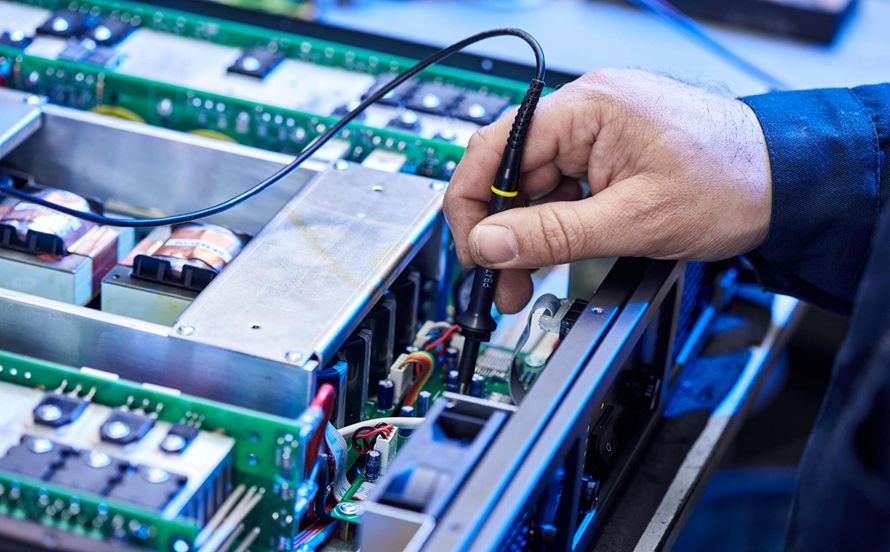
Power Integrity on a PCB: The PDN From Bulk to Die Power integrity is the least visible part of signal integrity and the most common cause of intermittent failures. A board can pass every eye diagram test and still reset a processor when an FPGA switches a thousand outputs at…
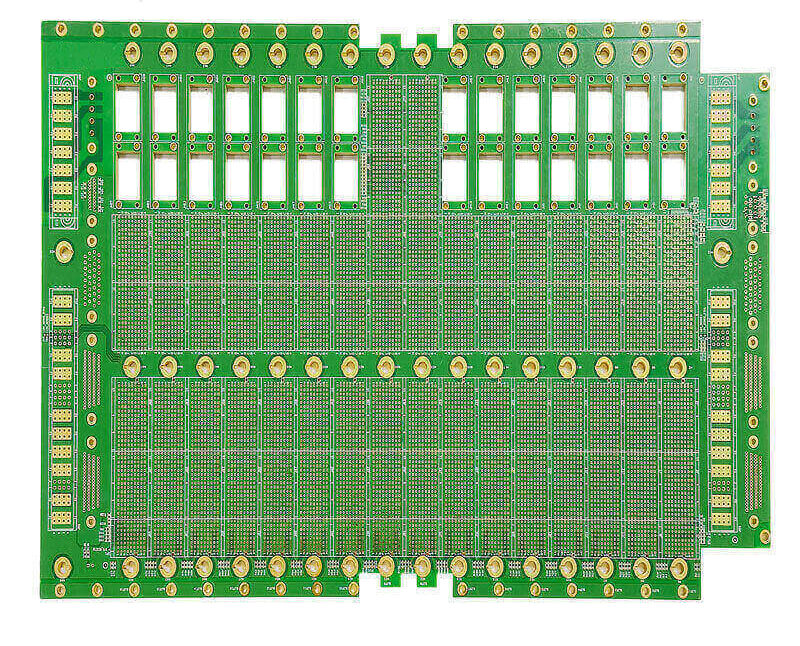
Backplane Design: Long Traces, Many Slots and Heavy Power A backplane is the board that carries the connectors for every card in a system. It usually has no active components of its own, it is physically large, and it is the most demanding board in the chassis in terms of…
PCB Edge Plating: Grounding, Shielding and Card Edges Edge plating is copper that wraps around the outside of a circuit board, connecting the surface layers to the edge of the board. It is used to ground a board to a chassis, to close the seam between a shield and an…
PCB Assembly Drawing: What It Has to Tell the Line An assembly drawing is the document that turns a design into a build instruction. The manufacturing data says where the copper goes and the centroid file says where the components sit, but neither of them explains what the assembly house…
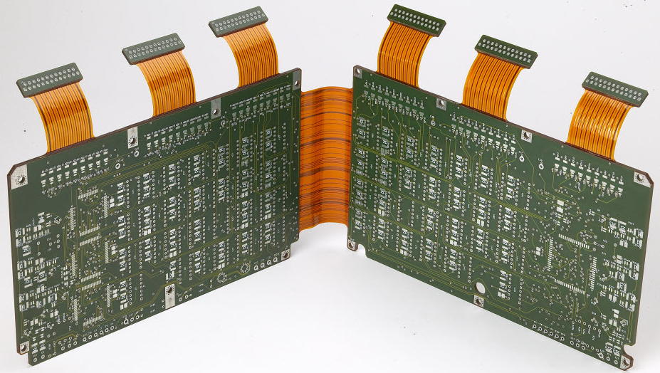
Flex PCB Bend Radius: Rules for a Circuit That Folds A flexible circuit is designed to be folded, and the number that decides whether it survives that fold is the bend radius. Specify it correctly and the flex behaves like a hinge for the life of the product. Get it…
Component Courtyards and Keepouts: Space the Process Needs Every component on a board needs space around it that carries no circuit. That space is what lets the stencil print, the nozzle place, the camera inspect and the technician rework, and it is the first thing a dense layout gives away.…
Solder Paste Volume: The Variable Behind Most Joint Problems If a single number predicted whether an assembly would pass inspection, it would be the volume of solder paste deposited on each pad. Every common joint defect – insufficient solder, bridging, tombstoning, solder balls – can be traced back to that…
ESD Protection Devices: Placement and Return Path An ESD protection device that is placed correctly protects a product for its whole life. The same device placed a few millimetres away from the connector, with a long ground connection, protects almost nothing, because the discharge finds a lower impedance path through…
Solder Joint Defects: Causes and How the Layout Prevents Them Most solder joint defects are decided long before the board reaches the reflow oven. A stencil aperture, a pad geometry, a mask clearance or a thermal connection can make a joint that is easy to produce or one that is…