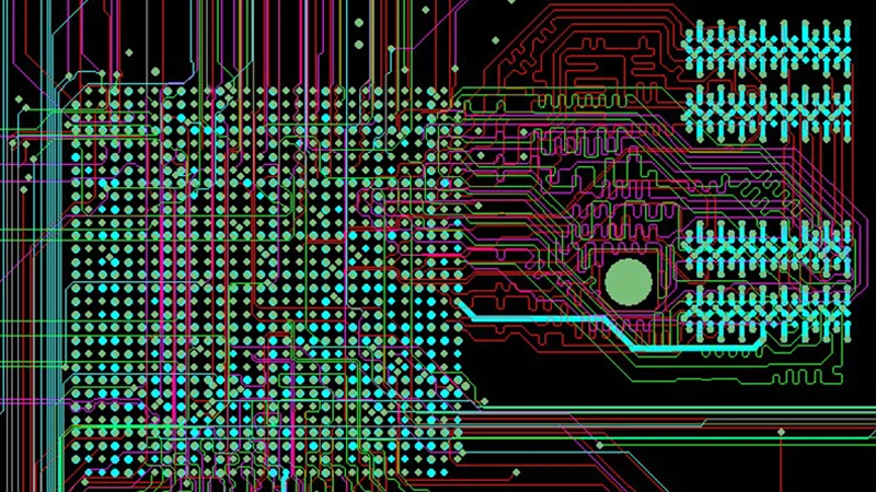
PCB Stackup Design: Layers, Planes and Symmetry Why the Stackup Comes First The stackup is the arrangement of copper layers and dielectric layers that the board will be built from, and it is decided before the routing, not after. Every signal layer needs a reference plane at a known distance,…

Via in Pad: Filling, Plating and Design Why Put a Via in a Pad Placing a via directly in a component pad solves two problems at once. It removes the short stub of trace that would otherwise run from the pad to a via placed beside it, which matters at…
PCB Panelisation: Tabs, Rails and Utilisation Why Boards Are Panelised A bare board is processed individually only in the smallest shops. Everywhere else the design is stepped into a panel so that a standard size sheet can carry many boards through imaging, plating, lamination, assembly and test on the same…
Backdrilling: Controlling Via Stubs The Stub Problem A through via connects the layers it is meant to connect, but it also continues to the opposite side of the board as an unused length of plated barrel. That unused length is the stub, and electrically it behaves as an open-ended transmission…
Stepped Cavities and Depth Control in PCB What a Stepped Cavity Is A stepped cavity is a recess milled into a board so that one area is thinner than the rest, without cutting all the way through. The result is a shelf at a controlled depth, used to sink a…
Press-Fit Connector Holes: Design Rules What Press-Fit Does A press-fit connector is inserted into plated holes without solder. The pin is slightly larger than the hole, and when it is pushed in, the elastic and plastic deformation of the pin and the barrel creates a gas-tight metal-to-metal contact that carries…
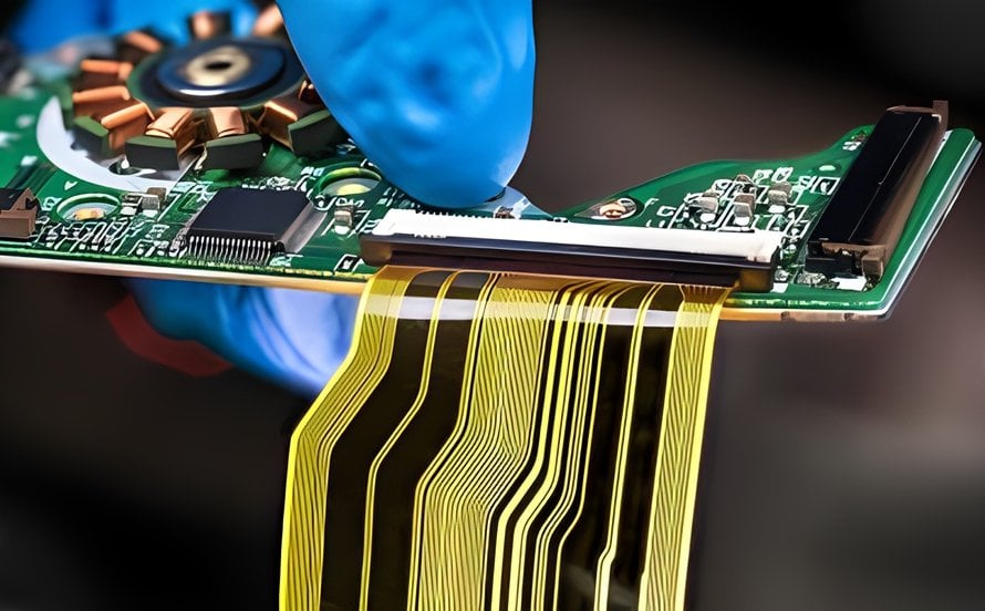
Copper Foil Types for Flexible Circuits Why Foil Type Matters Inside a Flex A flexible circuit bends, and the copper inside it has to survive thousands of cycles without cracking. That requirement puts the mechanical structure of the copper at the centre of the design, and the two foils in…
Blind, Buried and Through Vias Compared Three Ways to Cross a Stack A via exists to connect two layers, and the three types differ in which layers they reach. A through via passes through the entire board and is visible on both outer surfaces. A blind via starts on an…
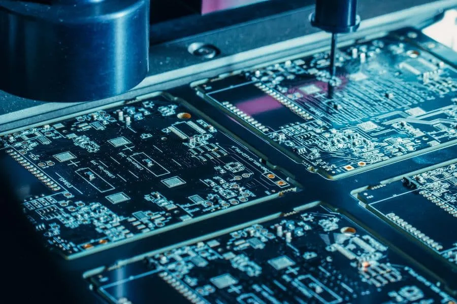
PCB Profiling: Routing, V-Score and Punching What Profiling Does Profiling is the step that separates the individual boards from the panel. It is one of the last operations in fabrication and one of the most consequential, because it sets the edge quality, the mechanical strength of the edge, the tolerance…
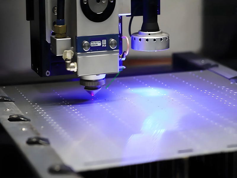
PCB Etching: Chemical Versus Laser Methods Two Ways to Remove Copper Etching is the step that turns a laminated copper sheet into conductors, and there are two practical ways to do it. Chemical etching dissolves unprotected copper in a bath, using a photoresist image as the mask. Laser etching removes…